TCP/IP core Offload Engine (TOE)
Introduction
The TCP/IPCore Offlead Engine (TOE) is a Hardwired TCP/IP embedded Ethernet controller that provides easier Internet connection to embedded systems. TOE enables users to have Internet connectivity in their applications by using the TCP/IP stack. WIZnet‘s Hardwired TCP/IP is the market-proven technology that supports TCP, UDP, IPv4, ICMP, ARP, IGMP, and PPPoE protocols. TOE embeds the 32Kbyte internal memory buffer for the Ethernet packet processing. Using TOE allows users to implement the Ethernet application by adding the simple socket program. It’s faster and easier than using any other Embedded Ethernet solutions. 8 independent hardware sockets can be used simultaneously. TOE also provides WOL (Wake on LAN) to reduce power consumption of the system.
Features
- Supports Hardwired TCP/IP Protocols : TCP, UDP, ICMP, IPv4, ARP, IGMP, PPPoE
- Supports 8 independent sockets simultaneously
- Supports Power down mode
- Supports Wake on LAN over UDP
- Internal 32Kbytes Memory for TX/RX Buffers
- Not supports IP Fragmentation
Functional description
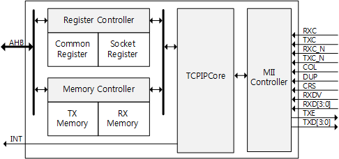
The below Figure shows the TOE block diagram.

TOE Memory map
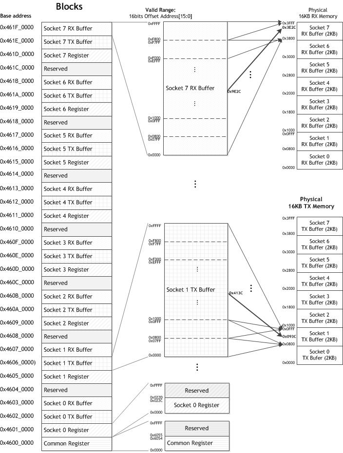
TOE has one Common Register Block, eight Socket Register Blocks, and TX/RX Buffer Blocks allocated to each Socket. The below Figure shows the selected block by the base address and the available offset address range of Socket TX/RX Buffer Blocks. Each Socket’s TX Buffer Block physically exists in one 16KB TX memory and is initially allocated with 2KB. Also, Each Socket’s RX Buffer Block physically exists in one 16KB RX Memory and is initially allocated with 2KB. Regardless of the allocated size of each Socket TX/RX Buffer, it can be accessible within the 16 bits offset address range (From 0x0000 to 0xFFFF). Refer to Memory for more information about 16KB TX/RX Memory organization and access method.

Common register map
Common Register Block configures the general information of TOE such as IP and MAC address. The below Table defines the offset address of registers in this block. Refer to Memory for more details about each register.
| Offset | Register |
|---|---|
| 0x0000 | TOE Version (VERSIONR) |
| 0x2000 | TICKCLOK (TCLKR) |
| 0x2100 | Interrupt (IR) |
| 0x2104 | Interrupt Mask (IMR) |
| 0x2108 | Interrupt Clear (IRCR) |
| 0x2110 | Socket Interrupt (SIR) |
| 0x2114 | Socket Mask (SIMR) |
| 0x2300 | Mode (MR) |
| 0x2400 | PPP Timer (PTIMER) |
| 0x2404 | PPP Magic (PMAGIC) |
| 0x2408 | PPP Destination MAC Address (PHAR1) |
| 0x240C | PPP Destination MAC address (PHAR0) |
| 0x2410 | PPP Session Identification (PSID) |
| 0x2414 | PPP Maximum Segment Size (PMSS) |
| 0x6000 | Source Hardware Address (SHAR1) |
| 0x6004 | Source Hardware Address (SHAR0) |
| 0x6008 | Gateway Address (GA) |
| 0x600C | Subnet Mask (SUB) |
| 0x6010 | Source IP Address (SIP) |
| 0x6020 | Network Configuration Lock (NCONFL) |
| 0x6040 | Retry Time (RTR) |
| 0x6044 | Retry Counter (RCR) |
| 0x6050 | Unreachable IP Address (UIP) |
| 0x6054 | Unreachable Port Address (UPORT) |
Socket register map
TOE supports 8 Sockets for communication channel. Each Socket is controlled by Socket n Register (n = 0,…,7 ,where n is socket number). < Table 2 > defines the 16bits Offset Address of registers in Socket n Register Block. Refer to Memory for more details about each register.
| Offset | Register |
|---|---|
| 0x0000 | Socket Mode (Sn_MR) |
| 0x0010 | Socket Command (Sn_CR) |
| 0x0020 | Socket Interrupt (Sn_IR) |
| 0x0024 | Socket Interrupt Mask (Sn_IMR) |
| 0x0028 | Socket Interrupt Clear (Sn_ICR) |
| 0x0030 | Socket Status (Sn_SR) |
| 0x0100 | Socket Protocol Number (Sn_PNR) |
| 0x0104 | Socket IP Type of Service (Sn_TOS) |
| 0x0108 | Socket TTL (Sn_TTLR) |
| 0x010C | Socket Fragment Offset (Sn_FRAG) |
| 0x0110 | Socket Maximum Segment (Sn_MSSR) |
| 0x0114 | Socket Port Number (Sn_PORT) |
| 0x0118 | Socket Destination Hardware address0 (Sn_DHAR0) |
| 0x011C | Socket Destination Hardware address1 (Sn_DHAR1) |
| 0x0120 | Socket Destination Port Number (Sn_DPORTR) |
| 0x0124 | Socket Destination IP Address (Sn_DIPR) |
| 0x0180 | Socket Keep Alive Timer (Sn_KATMR) |
| 0x0184 | Socket Retry Time (Sn_RTR) |
| 0x0188 | Socket Retry Counter (Sn_RCR) |
| 0x0200 | Socket TX Memory Size (Sn_TMSR) |
| 0x0204 | Socket TX Free Size (Sn_TXFSR) |
| 0x0208 | Socket TX Read Pointer (Sn_TXRDR) |
| 0x020C | Socket TX Write Pointer (Sn_TXWR) |
| 0x0220 | Socket RX Memory Size (Sn_TMSR) |
| 0x0224 | Socket RX Received Size (Sn_RSR) |
| 0x0228 | Socket RX Read Pointer (Sn_RXRDR) |
| 0x022C | Socket RX Write Pointer (Sn_RXWR) |
| 0x0400 | Socket TCP Status (Sn_TSR) |
Memory
TOE has one 16KB TX memory for Socket n TX Buffer Blocks and one 16KB RX memory for Socket n RX buffer Blocks.
16KB TX memory is initially allocated in 2KB size for each Socket TX Buffer Block (2KB X 8 = 16KB). The initial allocated 2KB size of Socket n TX Buffer can be re-allocated by using ‘Socket n TX Buffer Size Register (Sn_TXBUF_SIZE)’. Once all Sn_TXBUF_SIZE registers have been configured, Socket TX Buffer is allocated with the configured size of 16KB TX Memory and is assigned sequentially from Socket 0 to Socket 7. Its physical memory address is automatically determined in 16KB TX memory. Therefore, the total sum of Sn_TXBUF_SIZE should not exceed 16 in case of error in data transmission.
The 16KB RX memory allocation method is the same as the 16KB TX memory allocation method. 16KB RX memory is initially allocated into 2KB size for each Socket RX Buffer Block (2KB X 8 = 16KB). The initial allocated 2KB size of Socket n RX Buffer can be re-allocated by using ‘Socket n RX Buffer Size Register (Sn_RXBUF_SIZE)’.
When all Sn_RXBUF_SIZE registers have been configured, the Socket RX Buffer is allocated with the configured size in 16KB RX Memory and is assigned sequentially from Socket 0 to Socket 7. The physical memory address of the Socket RX Buffer is automatically determined in 16KB RX memory. Therefore, the total sum of Sn_RXBUF_SIZE should not exceed 16 or data reception error will occur.
For 16KB TX/RX memory allocation, refer to Sn_TXBUF_SIZE & Sn_RXBUF_SIZE in Socket register map . The Socket n TX Buffer Block allocated in 16KB TX memory is buffer for saving data to be transmitted by host. The 16bits Offset Address of Socket n TX Buffer Block has 64KB address space ranged from 0x0000 to 0xFFFF, and is configured with reference to ‘Socket n TX Write Pointer Register (Sn_TX_WR)’ & ‘Socket n TX Read Pointer Register(Sn_RX_RD)’. However, the 16bits Offset Address automatically converts into the physical address to be accessible in 16KB TX memory such as The upper Figure. Refer to [Socket register map](toe.md#socket register map) for Sn_TX_WR & Sn_TX_RD.
The Socket n RX Buffer Block allocated in 16KB RX memory is buffer for saving the received data through the Ethernet. The 16bits Offset Address of Socket n RX Buffer Block has 64KB address space ranged from 0x0000 to 0xFFFF, and is configured with reference to ‘Socket n RX RD Pointer Register (Sn_RX_RD)’ & ‘Socket n RX Write Pointer Register (Sn_RX_WR)’. However, the 16bits Offset Address automatically converts into the physical address to be accessible in 16KB RX memory such as The upper Figure. Refer to Socket register map for Sn_RX_RD & Sn_RX_WR.