System and Memory
System architecture
Main system consists of:
- Two masters:
- Cortex-M0 core
- uDMAC(PL230, 6 channels)
- Ten slaves
- Internal BOOT ROM
- Internal SRAM
- Internal Flash Memory
- Two AHB2APB bridge which connects all APB peripherals
- Four AHB dedicated to 16-bit GPIOs
- TCP/IP Hardware core
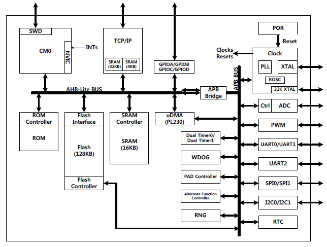
AHB-Lite BUS
- This bus connects the two masters (Cortex-M0 and uDMAC) and ten AHB slaves.
Two APB BUSs
- These buses connect Seventeen APB peripherals (Watchdog, two dual timers, pwm, two UARTs, simple UART, two SSPs, random number generator, real time clock, 12bits analog digital converter, clock controller, IO configuration, PAD MUX controller)
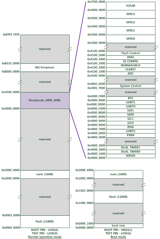
Memory organization
Program memory, data memory, registers and I/O ports are organized within the same linear 4-Gbyte address space. The bytes are coded in memory in Little Endian format. The lowest numbered byte in a word is considered the word’s least significant byte and the highest numbered byte the most significant.
Memory map
System Configuration Controller (SYSCFG)
Main purposes of the system configuration controller are the following
- Control of the memory remap feature
- The ability to enable an automatic reset if the system locks up
- Information about the cause of the last reset