Pad Controller (PADCON)
Introduction
Pads of W7500 are controllable. User can control pad’s characteristic.
Features
- W7500 have digital I/O pads and digital/analog mux I/O pads
- Controllable characteristics of pad are pull-up, pull-down, driving strength, input enable and CMOS/Schmitt trigger input buffer
- Each pad can be control individually by register.
Functional description
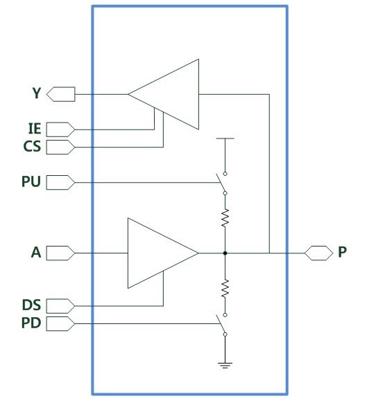
The below Figure shows the function schematic of digital I/O pad of W7500.

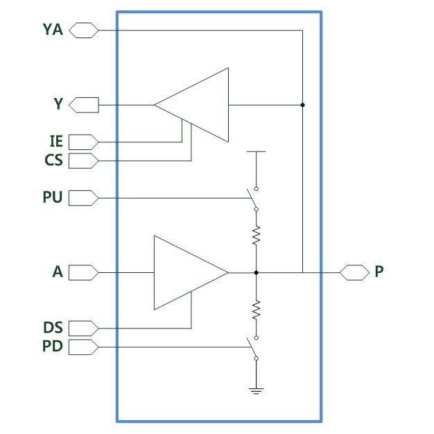
The below Figure shows the function schematic of digital/analog mux IO pad of W7500

Initials of Pad diagram is same as below.
P - PAD
YA – Analog Input (connect to ADC input)
Y – Digital Input
IE – Input buffer enable
| Condition | A | Y | P | |
|---|---|---|---|---|
| Input buffer enable (IE =1) | Output mode | OUT | OUT | OUT |
| Input mode | No use | IN | IN | |
| Input buffer enable (IE = 0) | Output mode | OUT | Low(0) | OUT |
| Input mode | No use | IN | IN | |
CS – CMOS/Schmitt trigger input buffer select
PU – Pull-up enable
A – Digital Output
DS – Driving strength select
| Condition | Rise/Fall Time(nSec) | Propagation Delay(nSec) | |||
|---|---|---|---|---|---|
| Driving Strength | Capacitance loading | Min | Max | Min | Max |
| High (DS = 1) | 25pF | 4 | 18 | 7 | 27 |
| 100pF | 11 | 53 | 11 | 44 | |
| Low (DS = 0) | 25pF | 1 | 8 | 4 | 16 |
| 100pF | 4 | 23 | 7 | ||
PD – Pull-down enable
User can set pad condition with IE, CS, PU/PD, DS by register.
And pads are can be controlled individually.