Datasheet
Hardware Specification
Product Spec Table
| Category | Description | |
|---|---|---|
| MCU (RP2040) | ARM Cortex-M0+ Dure Core | 133Mhz maximum frequency 264KB on-chip SRAM 16KB on-chip ROM 2MB External ROM 2 × UART, 2 × SPI controllers, 2 × I2C controllers, 16 × PWM channels 1 × USB 1.1 controller and PHY, with host and device support 8 × Programmable I/O (PIO) state machines for custom peripheral support |
| Ethernet (W5100S) | Hardwired TCP/IP With MAX and PHY | Support Hardwired Internet protocols: TCP, UDP, WOL over UDP, ICMP, IGMPv1/v2, IPv4, ARP, PPPoE Support 4 independent SOCKETs simultaneously Support SOCKET-less Command: ARP-Request, PING-Request Internal 16Kbytes Memory for TX/ RX Buffers 10BaseT/100BaseTX Ethernet PHY Integrated |
| Serial | Interface | UART (LVTTL 3.3V) SWD |
| Serial | Signal | TXD, RXD, RTS, CTS, DTR, DSR GND SWCLK, SWDIO |
| Serial | Parameters | Parity: None, Odd, Even Data bits: 7, 8 bit Flow control: None, RTS / CTS, XON / XOFF |
| Serial | Speed | TBD |
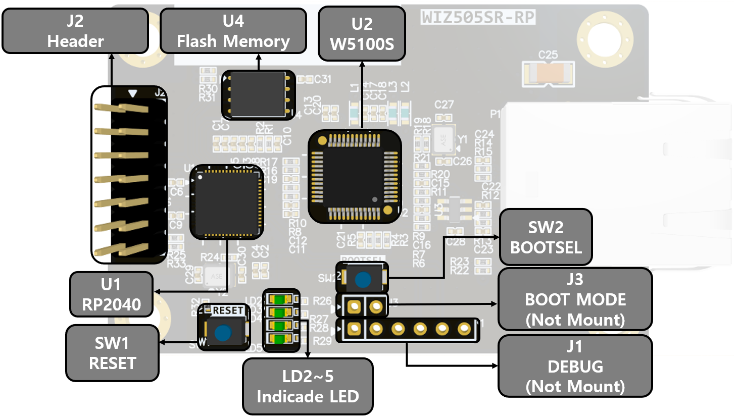
WIZ505SR-RP Callout
 |
| TOP |
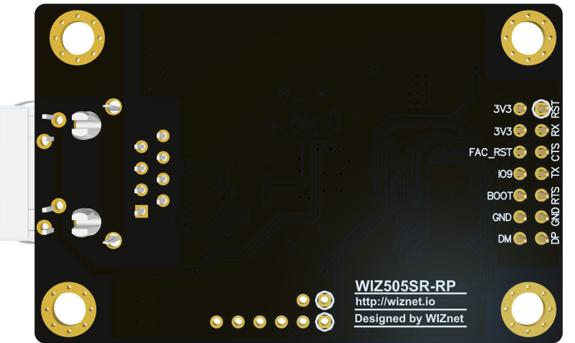 |
| BOTTOM |
Connector Specification
Magnetic rj45 modular jack (P1)
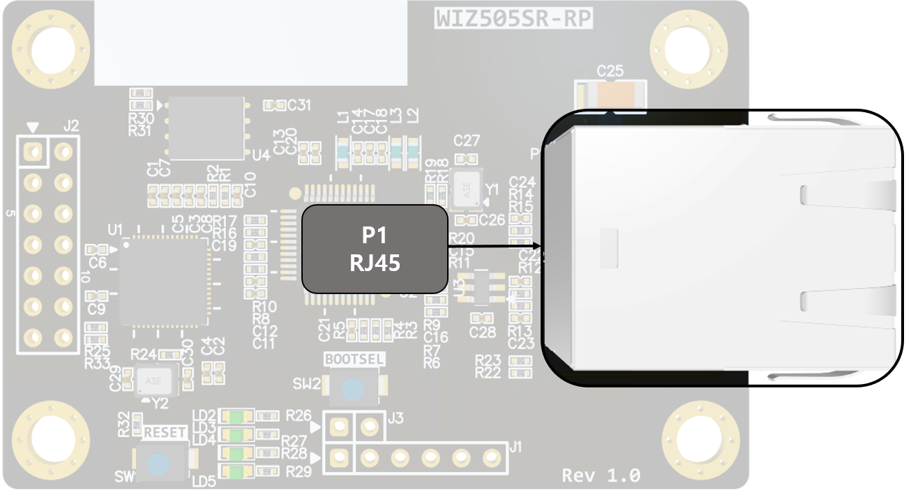
- If there is no Ethernet connection, the WIZ505SR-RP device will enter into a continuous reset loop.
2x7 UART1, Download (J2)
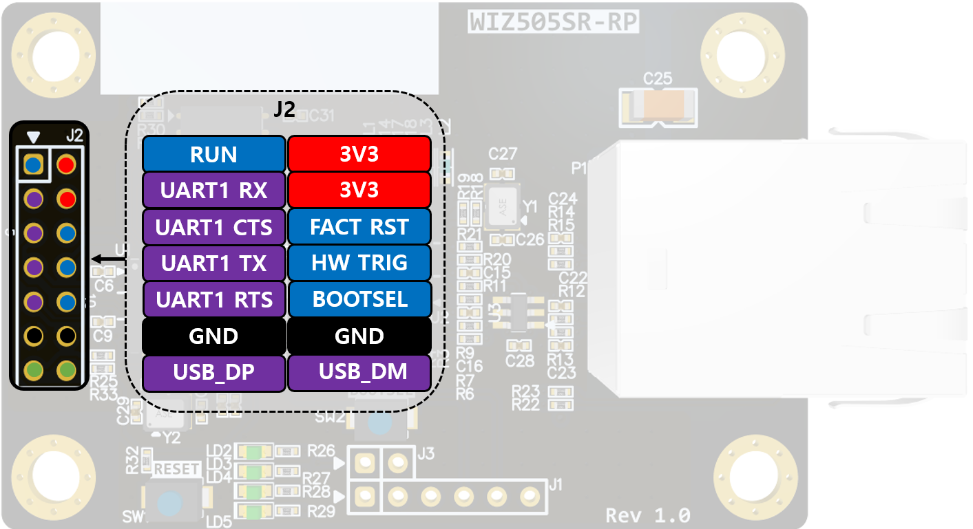
| Pin Number | Signal | Description |
|---|---|---|
| 1 | RUN | RP2040 Reset Signal Input Active Low |
| 2 | VCC | System Power Input (3.3V) |
| 3 | UART1_RX | UART1 RX |
| 4 | VCC | System Power Input (3.3V) |
| 5 | UART1_CTS | UART1 CTS |
| 6 | FACT RST | Factory Reset Signal input Drive this pin to Low for at least 5.0s then WIZ505SR-RP will be reset to factory settings |
| 7 | UART1 TX | UART1 TX |
| 8 | HW_TRIG | HW TRIG signal input Active Low High : Gateway Mode Low : AT Command Mode Changes will be reflected after reset |
| 9 | UART1_RTS | UART1 RTS |
| 10 | BOOTSEL | Active Low Drive this pin Low and reset(or power on),then RP2040 will enter USB Mass Storage Device mode Then RP2040 can be re-programming |
| 11 | GND | System Ground |
| 12 | GND | System Ground |
| 13 | USB_DP | USB DP signal input for RP2040 |
| 14 | USB_DM | USB DM Signal input for RP2040 |
1x6 UART0, SWD (J1)
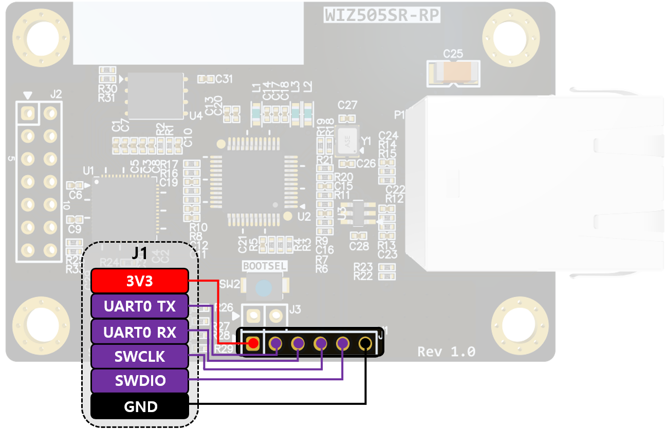
| Pin Number | Signal | Description |
|---|---|---|
| 1 | VCC | System Power input (3.3V) |
| 2 | TX | UART0_TX (Debug) |
| 3 | RX | UART0_RX (Debug) |
| 4 | SWCLK | SWDCLK |
| 5 | SWDIO | SWDIO |
| 6 | GND | System Ground |
J1 is not mounted connector
1x2 Boot mode select (J3)
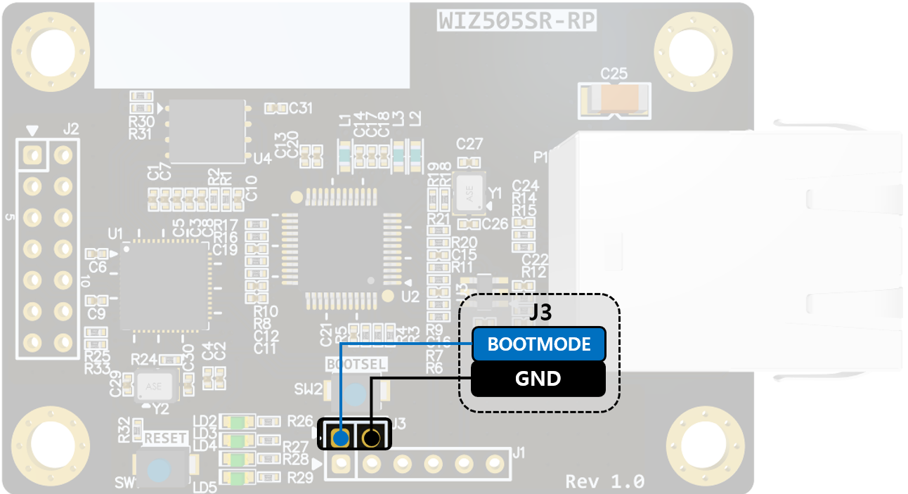
| Pin Number | Signal | Description |
|---|---|---|
| 1 | BOOTMODE | Boot Mode Select signal input Active Low Drive this pin low and reset(or power on),then WIZ505SR-RP will enter Boot mode |
| 2 | GND | System Ground |
J3 is not mounted connector
Switch Specification
RESET Switch (SW1)
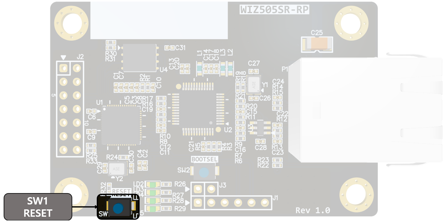
- Pressing SW1 will initiate a reset of the WIZ500SR-RP device.
BOOTSEL Switch (SW2)
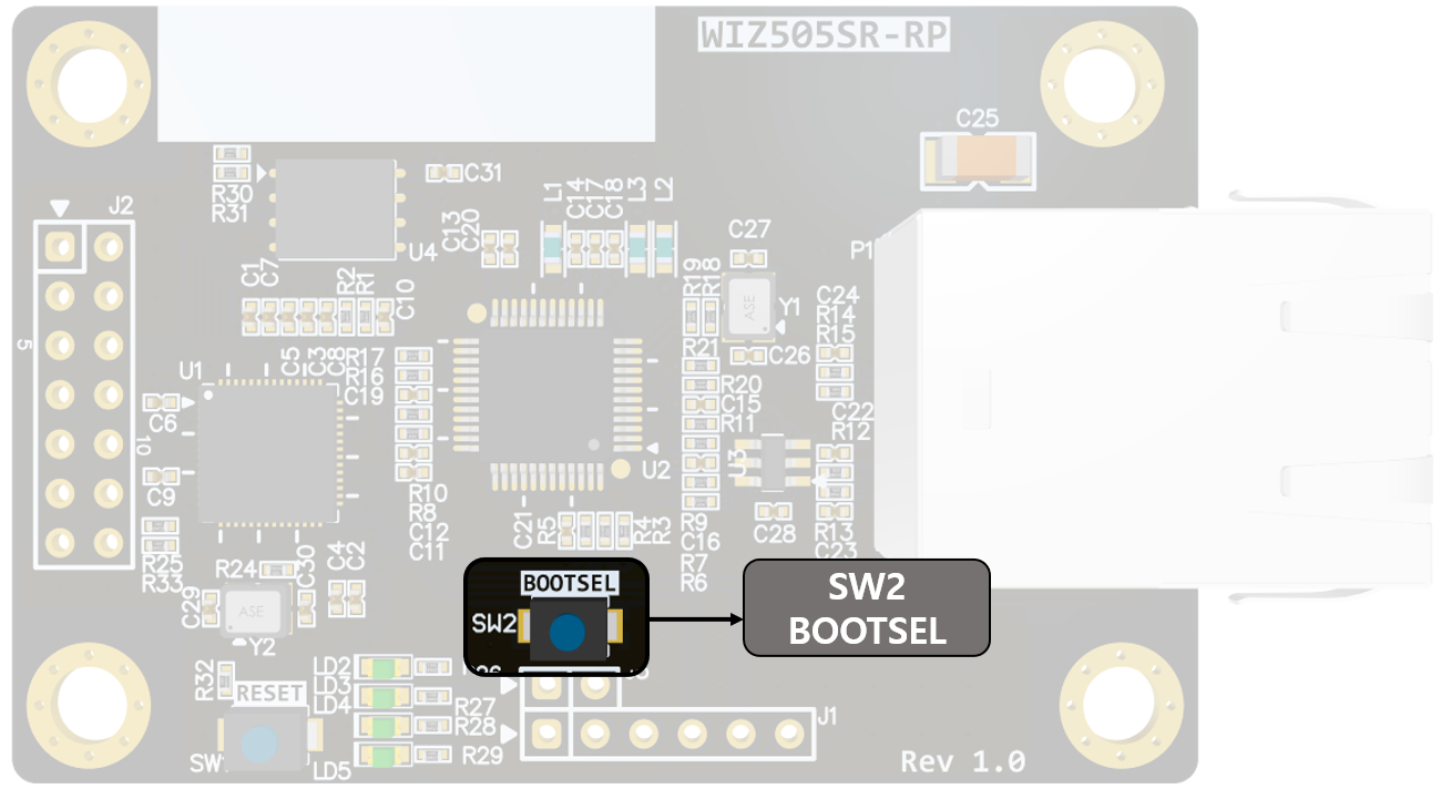
- Pressing SW2 and resetting (or powering on) will cause the RP2040 to enter USB Mass Storage Device mode. This enables the RP2040 to be reprogrammed.
WIZ505SR-RP indicators
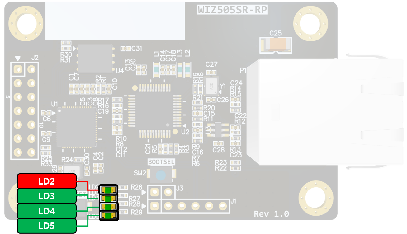
| Pin Number | Pin Name | Signal | Description |
|---|---|---|---|
| 1 | LD2 | Power LED(Red) | Power on LED |
| 2 | LD3 | TCP_STATUS LED(Green) | ON : Connect OFF : Disconnect |
| 3 | LD4 | LINK_STATUS LED(Green) | ON : LINK OFF : Unlink |
| 4 | LD5 | BLINK LED(Green) | Working indicate When Module working well Blinking every 1.0s |
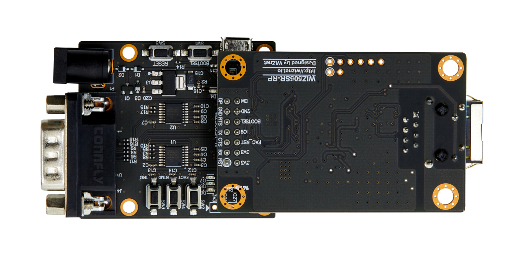
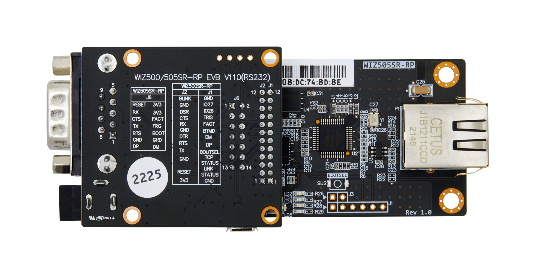
WIZ505SR-RP EVB
To utilize the WIZ505SR-RP EVB, connect the J1 connector of the WIZ505SR-RP to the J6 connector of the EVB.
 |
| TOP |
 |
| BOTTOM |
Schematic & Artwork
| H/W version | Type | Filetype | Download Link | Remarks |
|---|---|---|---|---|
| 1.0 | TTL | Altium | - | |
| ::: | ::: | - |
3D File
| H/W version | Type | Filetype | Download Link | Remarks |
|---|---|---|---|---|
| 1.0 | TTL | Altium | - |
Part list
| H/W version | Type | Filetype | Download Link | Remarks |
|---|---|---|---|---|
| 1.0 | TTL | Excel | - | |
| ::: | ::: | - |
Electrical Characteristics
Operating Conditions
| Symbol | Parameter | Min | Typ | Max | Unit |
|---|---|---|---|---|---|
| Vcc | Operating Voltage | 3.135 | 3.3 | 3.465 | V |
| Vss | Ground | 0 | 50 | mV | |
| fFCLK | Internal CPU clock frequency | - | - | 133 | MHz |
| Tstg | Storage Temperature (max) | -20 | 85 | ℃ | |
| TA | Ambient operating temperature | -20 | 85 | ℃ | |
| VIH | Input high voltage | 2.5 | V | ||
| VIL | Input low voltage | 0.6 | V | ||
| VOH | Output high voltage (High driving strength Current load = 6mA) (Low driving strength Current load = 3mA) | 2.83 | V | ||
| VOL | Output high voltage (High driving strength Current load = 6mA) (Low driving strength Current load = 3mA) | 0.32 | V |
Ethernet Power Dissipation
| Condition | Min | Typ | Max | Tol | Unit |
|---|---|---|---|---|---|
| 100M Transmitting | - | 125 | mA |
External Flash Memory
| Symbol | Parameter | Min | Unit |
|---|---|---|---|
| NEND | Sector Endurance | 100,000 | Cycles |
| TDR | Data Retention | 20 | Years |
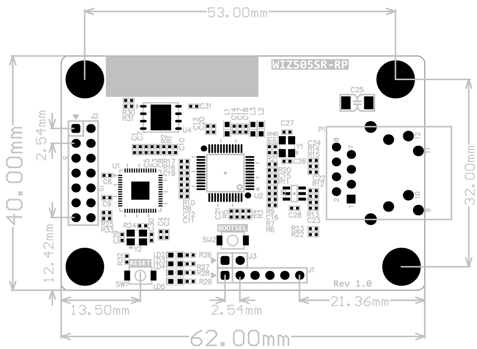
Dimensions
- WIZ505SR-RP Rev1.0 Dimension :
- 40mm x 62mm x 1.6mm ( PCB board size )
- 40mm x 66.5mm x 15mm ( Included part size )