WIZ850io
Overview
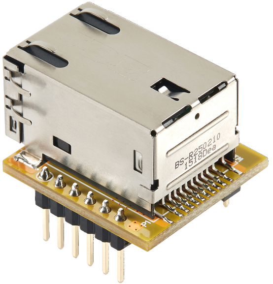
WIZ850io is a compact size network module that includes a W5500 (TCP/IP hardwired chip and PHY embedded), a transformer and RJ45. It can be used as a component and no effort is required to interface W5500 and Transformer. The WIZ850io is an ideal option for users who want to develop their Internet enabling systems rapidly. WIZ850io is hardware compatible with WIZ820io. WIZ820io users, to migrate to WIZ850io, need to modify the Firmware.
For the detailed information on implementation of Hardware TCP/IP, refer to the W5500 Datasheet.
Hardware Specification
WIZ850io
- Plugin Network Module.
- Hardware compatible with WIZ820io.
- Usable without H/W design for W5500, Transformer & RJ45.
- Fast evaluation for W5500 & MCU in the target board.
- Support high speed SPI interface.
- Support power down mode and Wake-on-LAN function
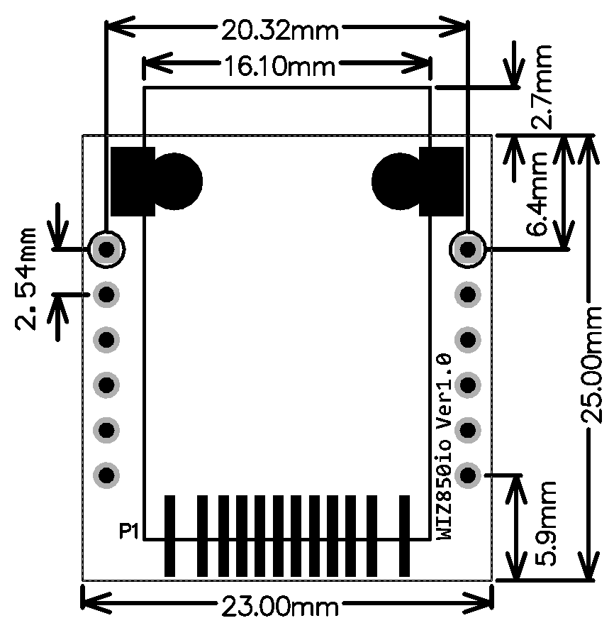
- Very small form factor : 23mm x 25mm x 18mm
- 1 x 6, 2.54mm Pin Header x 2
- Temperature : -40 ~ 85℃(Operation)
Pin Out
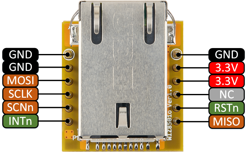
Pin Description
| Pin No. | Pin Type | Pin Name | Description | |
|---|---|---|---|---|
| J1 | 1 | P | GND | Ground |
| ::: | 2 | P | GND | Ground |
| ::: | 3 | I | MOSI | SPI Master Out Slave In This pin is used for SPI MOSI signal pin |
| ::: | 4 | I | SCLK | SPI Clock This pin is used for SPI Clock Signal pin |
| ::: | 5 | I | SCNn | SPI Slave Select This pin is used for SPI Slave Select Signal Pin when using SPI interface |
| ::: | 6 | I | INTn | W5500 Interrupt : Low activity This pin is used for indicating event like socket TCP connection, disconnection, data receiving timeout, WOL(Wake on Lan) and so on occurred in W5500 inside WIZ550io. The interrupt is cleared by writing IR register or Sn_IR. All interrupts are maskable. |
| Pin No. | Pin Type | Pin Name | Description | |
|---|---|---|---|---|
| J2 | 1 | P | GND | Ground |
| ::: | 2 | P | 3.3V | Power : 3.3V power supply |
| ::: | 3 | P | 3.3V | Power : 3.3V power supply |
| ::: | 4 | - | NC | Not Connect |
| ::: | 5 | I | RSTn | Reset : Low activity Hold at least 500us after asserted to LOW and keep HIGH until next Reset needed. |
| ::: | 6 | O | MISO | SPI Master In Slave Out This pin is used for SPI MISO signal pin |
User need to wait for 50ms after this pin is changed to HIGH to communicate with WIZ850io. (Refer to 5. Timing Diagram)
Characteristic
DC Characteristic
| Symbol | Parameter | Pins | Min | Typ | Max | Unit |
|---|---|---|---|---|---|---|
| VDD | Supply voltage | 3.3V | 2.97 | 3.3 | 3.63 | V |
| VIL | High level input voltage | ALL | 2.0 | 5.5 | V | |
| VIH | Low level input voltage | ALL | -0.3 | 0.8 | V | |
| VOL | Low level output voltage | ALL | 0.4 | V | ||
| VOH | High level output voltage | ALL | 2.4 | V | ||
| LOL | Low level output Current | ALL | 8.6 | 13.9 | 18.9 | mA |
| LOH | High level output Current | ALL | 12.5 | 26.9 | 47.1 | mA |
| IDD | Supply Current (Normal operation mode) | 3.3V | 132 | mA | ||
| LOH | Supply Current (Power Down mode) | 3.3V | 13 | mA |
Power Dissipation
| Condition | Min | Typ | Max | Unit |
|---|---|---|---|---|
| 100M Link | - | 128 | - | mA |
| 10M Link | - | 75 | - | mA |
| Un-Link (Auto-negotiation mode) | - | 65 | - | mA |
| 100M Transmitting | - | 132 | - | mA |
| 10M Transmitting | - | 79 | - | mA |
| Power Down mode | - | 13 | - | mA |
SPI Operations
As WIZ850io consists of W5500 and others, SPI operation of WIZ850io follows one of W5500. For more information about SPI operation of WIZ850io, please refer to W5500 Datasheet.
Timing Diagram
Reset Timing

| Symbol | Description | Min | Max |
|---|---|---|---|
| TRC | Reset Cycle Time | 500us | - |
| TPL | Internal Auto Configuration Time | - | 50ms |
SPI Timing
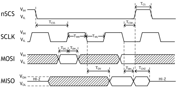
| Symbol | Description | Min | Max | Units |
|---|---|---|---|---|
| Fsck | SCLK Clock Frequency | - | 80 | MHz |
| TWH | SCLK High duration | 6 | - | ns |
| TWL | SCLK Low duration | 6 | - | ns |
| TCS | nSCS High duration | 5 | - | ns |
Schematic
- Revision 1.0 WIZ850io Rev1.0 Schematic(PDF)
- Revision 1.0 WIZ850io Rev1.0 Schematic(Altium)
- Revision 1.1 WIZ850io Rev1.0 Schematic(PDF)
- Revision 1.1 WIZ850io Rev1.0 Schematic(Altium)
Dimension
- WIZ850io V1.0 3D PDF :
Download
* This PDF must be run using the 'Adobe Acrobat'.