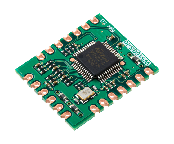
W5100S-io
We’ve Moved On!
This product has been discontinued as part of our ongoing commitment to innovation.
You can still access resources below.
Overview
W5100S-io is a compact size network module that includes a W5100S (TCP/IP hardwired chip and PHY embedded).It can be used as a component and no effort is required to interface W5100S. The W5100S-io an ideal option for users who want to develop their Internet enabling systems rapidly. W5100S-io is hardware compatible with W5500-io and W6100-io.
For the detailed information on implementation of Hardware TCP/IP, refer to the W5100S Datasheet.

Hardware Specification
W5100S-io
- Plugin Network Module.
- Hardware compatible with W5500-io, W6100-io.
- Usable without H/W design for W5100S.
- Fast evaluation for W5100S & MCU in the target board.
- Support high speed SPI interface.
- Support power down mode and Wake-on-LAN function
- Very small form factor : 20mm x 24mm x 2.6mm
Pin Out

Pin Description
| Pin No. | Pin Type | Pin Name | Description | |
|---|---|---|---|---|
| J1 | 1 | I | RX_P | RX_P |
| ::: | 2 | I | RX_N | RX_N |
| ::: | 3 | P | RCT | RX Center Tap This pin should be connect with external pulse transformer's RCT pin |
| ::: | 4 | P | TCT | TX Center Tap This pin should be connect with external pulse transformer's TCT pin |
| ::: | 5 | O | TX_P | TX_P |
| ::: | 6 | O | TX_N | TX_N |
| Pin No. | Pin Type | Pin Name | Description | |
|---|---|---|---|---|
| J2 | 1 | P | GND | Ground |
| ::: | 2 | P | GND | Ground |
| ::: | 3 | I | MOSI | Master Out Slave In This pin is used for SPI MOSI signal pin |
| ::: | 4 | I | SCLK | SPI clock input |
| ::: | 5 | I | CSn | Chip select input |
| ::: | 6 | O | INTn | Interrupt output Low: Interrupt asserted from W5100S High: No interrupt |
| ::: | 7 | O | LINK | LINK status output Low : Link High : Un Link |
| Pin No. | Pin Type | Pin Name | Description | |
|---|---|---|---|---|
| J3 | 1 | P | GND | Ground |
| ::: | 2 | P | 3.3V | Power : 3.3V power supply |
| ::: | 3 | P | 3.3V | Power : 3.3V power supply |
| ::: | 4 | - | NC | Not Connect |
| ::: | 5 | I | RSTn | Reset : Low activity Hold at least 500us after asserted to LOW and keep HIGH until next Reset needed. |
| ::: | 6 | O | MISO | SPI Master In Slave Out This pin is used for SPI MISO signal pin |
| ::: | 7 | O | ACTn | Active LED Low: Carrier sense from the active PMD High: No carrier sense |
Characteristic
DC Characteristic
| Symbol | Parameter | Pins | Min | Typ | Max | Unit |
|---|---|---|---|---|---|---|
| VDD | Supply voltage | 3.3V | 2.97 | 3.3 | 3.63 | V |
| VIL | High level input voltage | ALL | 2.0 | 5.5 | V | |
| VIH | Low level input voltage | ALL | -0.3 | 0.8 | V | |
| VOL | Low level output voltage | ALL | 0.4 | V | ||
| VOH | High level output voltage | ALL | 2.4 | V | ||
| LOL | Low level output Current | ALL | 8.6 | 13.9 | 18.9 | mA |
| LOH | High level output Current | ALL | 12.5 | 26.9 | 47.1 | mA |
| IDD | Supply Current (Normal operation mode) | 3.3V | 132 | mA | ||
| LOH | Supply Current (Power Down mode) | 3.3V | 13 | mA |
Power Dissipation
| Condition | Min | Typ | Max | Unit |
|---|---|---|---|---|
| 100M Link | - | 93 | 110 | mA |
| 10M Link | - | 93 | 210 | mA |
| Un-Link (Auto-negotiation mode) | - | 43 | 170 | mA |
| Power Down mode | - | 10 | 20 | mA |
SPI Operations
As W5100S-io consists of W5100S and others, SPI operation of W5100S-io follows one of W5100S. For more information about SPI operation of W5100S-io, please refer to W5100S Datasheet.
Schematic & Artwork
Module
- Revision 1.0 W5100S-io V100 Schematic(PDF)
- Revision 1.0 W5100S-io V100 Schematic(Altium)
Reference Schematic
- Revision 1.0 W5100s-io V100 Reference Schematic(PDF)
3D File
Part list
- Revision 1.0 W5100S-io V100 Part list(PDF)
- Revision 1.0 W5100S-io V100 Part list(Excel)
Dimension
- W5100S-io V100 Dimension
- 24mm x 20mm x 1.0mm ( PCB board size )
- 24mm x 20mm x 2.6mm ( Included part size )
