Datasheet
1. Introduction
WizFi250 is a small size wireless module for the highest level of
integration, featuring 802.11b/g and 802.11n.
It includes a 2.4 GHz WLAN CMOS power amplifier (PA) that meets the
output power requirements of most handheld systems.
Along with the integrated power amplifier, the WizFi250 also includes
integrated transmit and receive baluns, further reducing the overall
solution cost.
The small size and low profile physical design eases enabling high
performance wireless connectivity without space constraint in system
designs.
Hardware WAPI acceleration engine, AES, TKIP, WPA and WPA2 are supported
to provide your network with the latest security requirements.
For software and driver development, WIZnet provides extensive technical
documents and reference software codes for system integration.
2. Features
- Single band 2.4GHz IEEE 802.11b/g/n
- Integrated RF power amplifier
- Supports wireless data rates up to 65Mbit/s
- 1MB Flash Memory, 128KB SRAM, 1MB Serial Flash
- Supports per packet Rx Antenna diversity
- Low power consumption & excellent power management performance to extend battery life.
- Small size, suitable for low volume system integration.
- Easy integration into mobile and handheld devices flexible system configuration.
- 2.412-2.484 GHz two SKUs for worldwide market.
- Lead Free design supporting Green design requirements, RoHS Compliance.
- Device Package : 28x20 mm (17x20 mm)
- Serial Interface : UART, SPI
- Powerful Web server provides
- Soft AP
- Sufficient memory retention
- Wi-Fi Security (WEP, WPA/WPA2PSK)
- L2 Switching
- OTA(Over The Air F/W Upgrading)
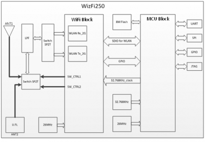
3. Block diagram
The WizFi250 module is designed based on WiFi block and MCU block . It supports generic SPI, UART interface to connect WLAN to the host processor. A simplified block diagram of the WizFi250 module is depicted in the Fig. below.
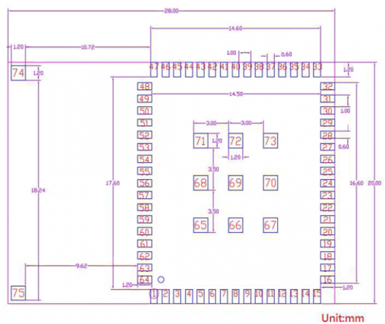
4. Pin description
Pin map
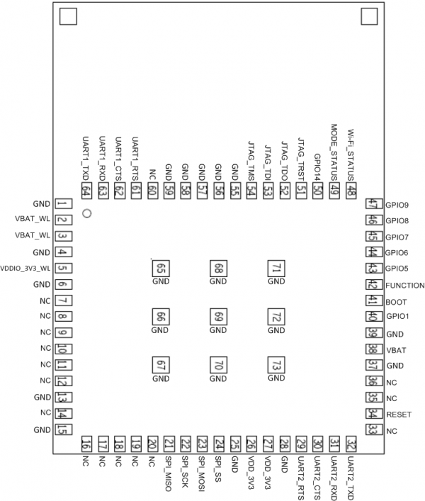
Pin description
| Pin Number | Pin Define | Type | Description |
|---|---|---|---|
| 1 | GND | - | Groud |
| 2 | VBAT_WL | I | Battery supply input |
| 3 | VBAT_WL | I | Battery supply input |
| 4 | GND | - | Ground |
| 5 | VDDIO_3V3_WL | I | Digital I/O supply. |
| 6 | GND | - | Ground |
| 7 | NC | - | -- |
| 8 | NC | - | -- |
| 9 | NC | - | -- |
| 10 | NC | - | -- |
| 11 | NC | - | -- |
| 12 | NC | - | -- |
| 13 | GND | - | Ground |
| 14 | NC | - | -- |
| 15 | GND | - | Ground |
| 16 | NC | - | -- |
| 17 | NC | - | -- |
| 18 | NC | - | -- |
| 19 | NC | - | -- |
| 20 | NC | - | -- |
| 21 | SPI_MISO | I/O | SPI Master In Slave Out |
| 22 | SPI_SCK | I/O | SPI Clock |
| 23 | SPI_MOSI | I/O | SPI Master Out Slave In |
| 24 | SPI_SS | I/O | SPI Slave Select |
| 25 | GND | - | Ground |
| 26 | VDD_3V3 | I | Power supply for I/O and the internal regulator |
| 27 | VDD_3V3 | I | Power supply for I/O and the internal regulator |
| 28 | GND | - | Ground |
| 29 | UART2_RTS | I/O | Active-low request-to-send signal for UART2 interface (Not Used) |
| 30 | UART2_CTS | I/O | Active-low clear-to-send signal for UART2 interface (Not Used) |
| 31 | UART2_RXD | I | Serial data input for UART2 interface (Not Used) |
| 32 | UART2_TXD | O | Serial data output for UART2 interface (Not Used) |
| 33 | NC | - | -- |
| 34 | RESET | I | RESET pin (Active Low) |
| 35 | NC | - | -- |
| 36 | NC | - | -- |
| 37 | GND | - | Ground |
| 38 | VBAT | I | Power supply when VDD_3V3 is not present. |
| 39 | GND | - | Ground |
| 40 | GPIO1 | I/O | GPIO1 pin |
| 41 | BOOT | I | BOOT MODE pin (Active low) |
| 42 | FUNCTION | I | FUNCTION pin (Active Low) |
| 43 | GPIO5 | I/O | GPIO5 pin |
| 44 | GPIO6 | I/O | GPIO6 pin |
| 45 | GPIO7 | I/O | GPIO7 pin |
| 46 | GPIO8 | I/O | GPIO8 pin |
| 47 | GPIO9 | I/O | GPIO9 pin |
| 48 | Wi-Fi_STATUS | I/O | Wi-Fi Status pin |
| 49 | MODE_STATUS | I/O | MODE Status pin |
| 50 | SPI_Data_Ready(GPIO14) | I/O | In SPI Mode, It is used to SPI_Data Ready Pin |
| 51 | JTAG_TRST | I | For normal operation, if JTAG is not used, this pin can be left unconnected (NC) |
| 52 | JTAG_TDO | I/O | For normal operation, if JTAG is not used, this pin can be left unconnected (NC) |
| 53 | JTAG_TDI | I/O | For normal operation, if JTAG is not used, this pin can be left unconnected (NC) |
| 54 | JTAG_TMS | I | For normal operation, if JTAG is not used, this pin can be left unconnected (NC) |
| 55 | JTAG_TCK | I | For normal operation, if JTAG is not used, this pin can be left unconnected (NC) |
| 56 | GND | - | Ground |
| 57 | GND | - | Ground |
| 58 | GND | - | Ground |
| 59 | GND | - | Ground |
| 60 | NC | - | -- |
| 61 | UART1_RTS | I/O | Active-low request-to-send signal for UART1 interface (Use) |
| 62 | UART1_CTS | I/O | Active-low clear-to-send signal for UART1 interface (Use) |
| 63 | UART1_RXD | I | Serial data input for UART1 interface (Use) |
| 64 | UART1_TXD | O | Serial data output for UART1 interface (Use) |
| 65~73 | GND | - | Ground |
5. Technical Specification
Absolute maximum rating
| Supply Power | Max +3.6 Volt | |
|---|---|---|
| Storage Temperature | - 40° to 85° Celsius | |
| Voltage ripple | +/- 2% Max | Values not exceeding Operating voltage |
Recommended operation condition
Temperature, humidity
The WizFi250 can withstand the operational requirements as listed in the table below.
| Operating Temperature | -20° to 85° Celsius |
|---|---|
| Humidity range | Max 95%, Non condensing, relative humidity |
- The maximum operating ambient temperature can be up to 85°. Exposure to absolute-maximum-rated conditions may cause performance degradation and affect device reliability. For the best performance -20° to 75° is recommended.
Voltage
Power supply for the WizFi250 module will be provided by the host via power pins.
| Symbol | Parameter | Min | Typ. | Max | Unit |
|---|---|---|---|---|---|
| VBAT_WL | power supply for WizFi250 | 3.0 | 3.3 | 3.6 | V |
| VDDIO_3V3_WL | host Interface power supply | 3.0 | 3.3 | 3.6 | V |
| VBAT_MICRO | backup operating voltage | 3.0 | 3.3 | 3.6 | V |
| VDD_3V3 | power supply for MCU | 3.0 | 3.3 | 3.6 | V |
Current consumption
The WizFi250 on operation output current consumption :
| MCU mode | WiFi mode (802.11n) | Typ. (RMS) | Max. |
|---|
| Normal mode | Not Associated | 14 mA | 18 mA |
| Normal mode | Associated | 67 mA | 69 mA |
| Normal mode | Associated (IEEE Power Save mode) | 32 mA | 65 mA |
| Stop mode | Associated (IEEE Power Save mode) | 14 mA | 17 mA |
| Stop mode | Not Associated | 3 mA | 23 mA |
The WizFi250 on TX mode output current consumption :
(Typical spec is defined @3.3V 25℃ ; MAX. spec is defined @3.0V 70℃)
| Current Consumption | Typ. | Max. |
|---|---|---|
| Tx output power @16.5 dBm on 11b 1M | 385 mA | 430 mA |
| Tx output power @ 16.5 dBm on 11b 11M | 370 mA | 410 mA |
| Tx output power @ 15 dBm on 11g 6M | 345 mA | 380 mA |
| Tx output power @ 13 dBm on 11g 54M | 290 mA | 320 mA |
| Tx output power @ 14.5 dBm on 11n MCS0 | 315 mA | 350 mA |
| Tx output power @ 12 dBm on 11n MCS7 | 265 mA | 295 mA |
The WizFi250 on RX mode current consumption :
(Typical spec is defined @3.3V 25℃; MAX. spec is defined @3.0V 70℃)
| Current Consumption | Typ. | Max. |
|---|---|---|
| Rx @ 11b 1M | 120 mA | 150 mA |
| Rx @ 11b 11M | 120 mA | 150 mA |
| Rx @ 11g 6M | 120 mA | 150 mA |
| Rx @ 11g 54M | 120 mA | 150 mA |
| Rx @ 11n MCS0 | 120 mA | 150 mA |
| Rx @ 11n MCS7 | 120 mA | 150 mA |
Wireless specifications
WizFi250 complies with following features and standards;
| Features | Description | |
|---|---|---|
| WLAN Standards | IEEE 802 11 b/g/n | |
| Antenna Connecter Port | One printed antenna, one U.FL connector for external antenna | |
| Frequency Band | 2.400 GHz ~ 2.484 GHz | |
| Number of Sub Channels | CH1 to CH14 | |
| Modulation | DSSS, CCK, OFDM, BPSK, QPSK,16QAM, 64QAM | |
| Supported data rates | 11b | 1, 2, 5.5, 11 (Mbps) |
| ::: | 11g | 6, 9, 12, 18, 24, 36, 48, 54 (Mbps) |
| ::: | 11n | HT20 MCS0(6.5Mbps) to HT20 MCS7(65Mbps) |
Specifications of WiFi’s output power, evm, sensitivity
The WizFi250 WiFi output power is listed in the table below:
| Characteristics | Typ. | Criteria | Unit | |
|---|---|---|---|---|
| RF Average Output Power, 802.11b CCK Mode | 1M | 16.5 | +/- 1.5 | dBm |
| ::: | 11M | 16.5 | +/- 1.5 | dBm |
| RF Average Output Power, 802.11g OFDM Mode | 6M | 15 | +/- 1.5 | dBm |
| ::: | 54M | 13 | +/- 1.5 | dBm |
| RF Average Output Power, 802.11n OFDM Mode | MCS0 | 14.5 | +/- 1.5 | dBm |
| ::: | MCS7 | 12 | +/- 1.5 | dBm |
WiFi TX EVM following the IEEE spec as listed in the table below:
| Characteristics | IEEE Spec | Unit | |
|---|---|---|---|
| RF Average Output EVM (11b) | @1 Mbps | -10 | dB |
| ::: | @11 Mbps | -10 | dB |
| RF Average Output EVM (11g) | @6 Mbps | -5 | dB |
| ::: | @54 Mbps | -25 | dB |
| RF Average Output EVM (11n) | @ MCS0 | -5 | dB |
| ::: | @ MCS7 | -28 | dB |
The WizFi250 Wi-Fi sensitivity as listed in the table below:
| Receiver Characteristics | Typ. | Max. | Unit |
|---|---|---|---|
| PER < 8%, Rx Sensitivity @ 1 Mbps | -96 | -89 | dBm |
| PER < 8%, Rx Sensitivity @ 11 Mbps | -88 | -84 | dBm |
| PER < 10%, Rx Sensitivity @ 6 Mbps | -90 | -83 | dBm |
| PER < 10%, Rx Sensitivity @ 54 Mbps | -74 | -70 | dBm |
| PER < 10%, Rx Sensitivity @ MCS0 | -89 | -83 | dBm |
| PER < 10%, Rx Sensitivity @ MCS7 | -71 | -67 | dBm |
6. I/O port characteristics
WizfFi250 is a small size wireless module. Unless otherwise specified,
parameters are given as in the table below.
^Symbol^ Parameter ^Conditions^ Min ^Typ^ Max ^Unit^
| VIL | Standard IO input low level voltage | -0.3 | 0.28*(VDD-2V)+0.8V | V | ||
| ::: | IO FT(1) input low level voltage | -0.3 | 0.32*(VDD-2V)+0.75V | V | ||
| VIH | Standard IO input high level voltage | 0.41*(VDD-2V)+1.3V | VDD+0.3 | V | ||
| ::: | IO FT(1) input high level voltage | VDD > 2V | 0.42*(VDD-2V)+1V | 5.5 | V | |
| ::: | ::: | VDD≤ 2V | 5.2 | |||
| Vhys | Standard IO Schmitt trigger voltage hysteresis(2) | 200 | mV | |||
| ::: | IOFT Schmitt trigger voltage hysteresis(2) | 5%VDD(3) | mV | |||
| Ilkg | Input leakage current(4) | VSS≤VIN≤VDD Standard I/Os | ±1 | μA | ||
| ::: | ::: | VIN=5V,I/O FT | 3 | |||
| RPU | Weak pull-up equivalent resistor(5) | VIN=VSS | 30 | 40 | 50 | k Ω |
| RPD | Weak pull-down equivalent resistor(5) | VIN=VDD | 30 | 40 | 50 | k Ω |
| CIO | I/O pin capacitance | 5 | pF |
1. FT = Five-volt tolerant. In order to sustain a voltage higher than
VDD+0.3 the internal pull-up/pull-down resistors must be
disabled.
2. Hysteresis voltage between Schmitt trigger switching levels. Based
on characterization, not tested in production.
3. With a minimum of 100 mV.
4. Leakage could be higher than max. if negative current is injected on
adjacent pins.
5. Pull-up and pull-down resistors are designed with a true resistance
in series with a switchable PMOS/NMOS. The MOS/NMOS contribution to the
series resistance is minimum(~10% order).
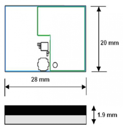
7. Dimensions, weight and mounting
The following paragraphs provide the requirements for size, weight and
mounting of the WizFi250.
Dimensions
WizFi250-PA
- 28 mm (W) x 20 mm (L) x 1.9 mm (H) (+/- 0.1mm) (PCB Antenna,
Including metal shielding)
WizFi250-CON
- 17 mm (W) x 20 mm (L) x 1.9 mm (H) (+/- 0.1mm)
Pin out and pin description
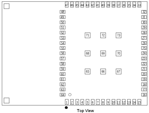
Recommend footprint
8. Design Guide
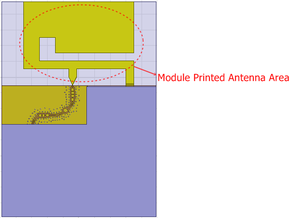
PCB Antenna Guide
Module Location Recommendation
To get better antenna performance, the following two module locations
are advised.

-Location 1: Module is recommended to be on the upper right corner of
main board.

-Location 2: Module is recommended to be on the upper left corner of
main board.
Module Layout Guideline
- Main board antenna area under module printed antenna should be clear
or empty.
- No signals, GND or power traces can be routed in antenna area for
each layers of the main board.
- Any mental lids, power traces or metal components should be placed
far away from the antenna area on the main board.
- Keep GND plane as large as you can on main board.
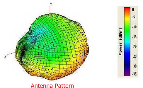
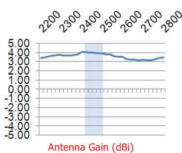
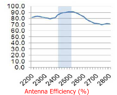
Antenna Simulation Result
| Ant. on right-up corner | Ant. on left-up corner | |
|---|---|---|
| Configuration |  |  |
| S11 | 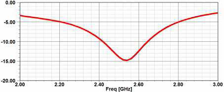 | 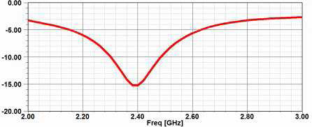 |
| Gain | 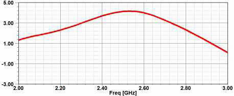 | 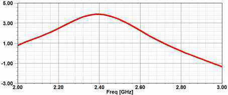 |
| 3D Pattern | 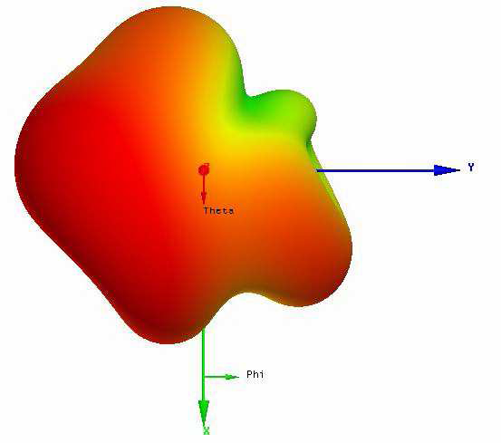 | 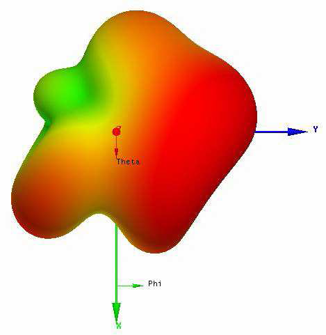 |
Antenna Measurement Setup
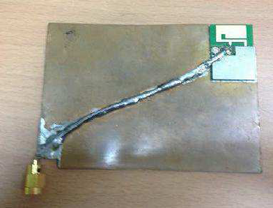
Module is on the upper right corner of main board for performance
measurement.
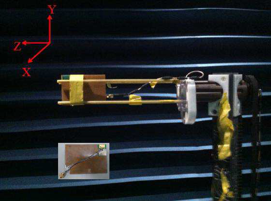
Antenna measurement setup as the figure.
Antenna Measurement Results
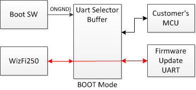
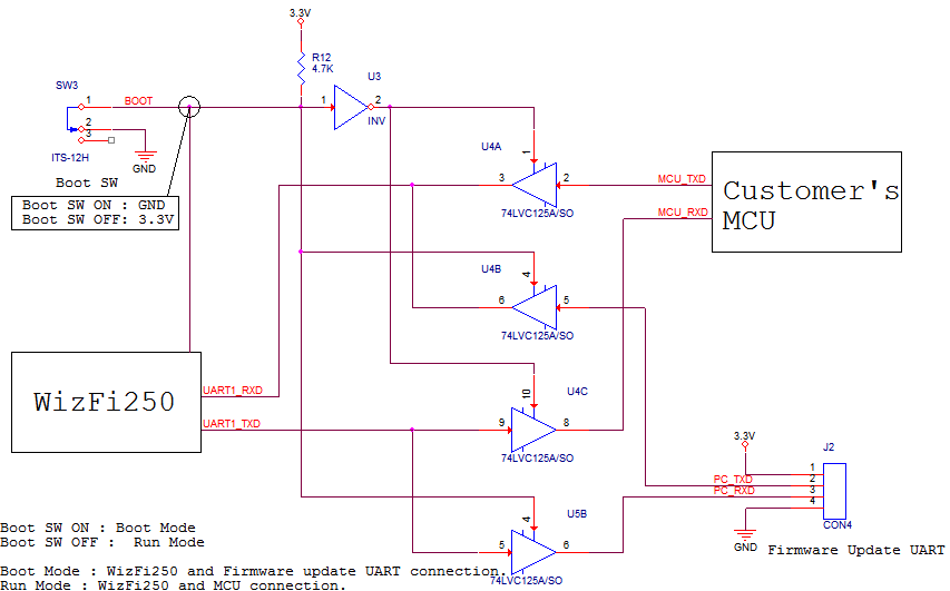
Firmware Update - Circuit Guide
WizFi250 provides some specific functions according to its firmware. Until now, there is a
standard firmware and some customized firmware to specific customers
available. It is possible to perform firmware updates.
WizFi250 decides its operating mode according to the input value of the
BOOT signal. WizFi250 operates in boot mode when the BOOT input value is
“LOW”, otherwise it operates in the standard run mode. WizFi250
communicates with a PC via UART in order to upload another firmware, so
you have to connect UART1_RXD and UART1_TXD to the external interface
for communicating with PC.
Two different schematics for that connection are listed below.
Case 1
A simple circuit for updating firmware.
If your application MCU has UART communication with WizFi250, there is a
possibility that the firmware update with an external PC will fail
because of dual use of the one UART interface. In that case WIZnet
cannot guarantee a completely successful update.
Therefore, please monitor the signal of BOOT with your MCU by a GPIO.
Please stop the UART communication between your MCU and the WizFi250
when the BOOT input value is “LOW”. After that detection of a "LOW" BOOT
signal you can succeed firmware update.

Case 2
This circuit selects the UART communication using some extra hardware. If the BOOT SW is ON(GND), it is in BOOT Mode, and if the BOOT SW is OFF(3.3V) it is RUN Mode. The UART signal of the WizFi250 is connected to the firmware update UART (PC) when it becomes BOOT Mode, so firmware updates are made possible. The UART signal of the WizFi250 is only connected on your MCU if the BOOT signal is "High" and WizFi250 goes into the RUN Mode.

9. Recommended reflow profile
The following paragraphs provide the requirements for the size, weight and mounting of the WizFi250.
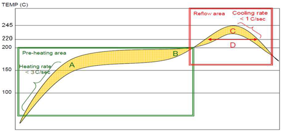
A-B. Temp.: 150-200℃; soak time:60-120sec.
C. Peak temp: 235~245℃.
D. Time above 220 ℃: 40~90sec.
Suggestion: Optimal cooling rate is <1℃/sec. from peak to 220 ℃.
10. WizFi250 Ref. Schematic
Ref SchematicInstruction to OEM
This device complies with Industry Canada’s licence-exempt RSSs. Operation is subject to the following two conditions:
(1) This device may not cause interference; and
(2) This device must accept any interference, including interference
that may cause undesired operation of the device.
This application and its antenna must not be co-located or operation in conjunction with any other antenna or transmitter. A minimum separation distance of 20cm must be maintained between the antenna and the person for this appliance to satisfy the RF exposure requirements.
Host labeling requirement: "Contains transmitter module IC: 20560-WIZFI250"