Electrical Characteristics
Absolute maximum ratings
These are stress ratings only and functional operation of the device at these conditions is not implied. Exposure to maximum rating conditions for extended periods may affect device reliability.
Voltage Characteristics
| Symbol | Ratings | Min | Max | Unit |
|---|---|---|---|---|
| VDD-VSS | External main supply voltage (VDD) | -0.3 | 3.6 | V |
| VIN | Input voltage on IO pins | VSS - 0.3 | 3.6 | V |
| SVDDH | I/O Power on slope | 3.3V/Sec | 1V/uSec | - |
| △VSS | Variations between difference VDD power pins | 50 | mV | |
| △VDD | Variations between different ground pins | 50 | mV |
Current Characteristics
| Symbol | Ratings | Max | Unit |
|---|---|---|---|
| IVDDsUM | Total current into sum of all VDD power lines (source) | 100 | mA |
| IVDD | Maximum current into each ADD power pin (source) | 90 | mA |
| IIO_PAD | Total output current sunk by sum of all IOs and control pins | 75 | mA |
| IINJ_PAD | Single pin input injected current | ±10 | mA |
| IINJ_SUM | Sum of all input injected current | ±50 | mA |
Thermal Characteristics
| Symbol | Ratings | Min | Max | Unit |
|---|---|---|---|---|
| TStorge | Storage temperature range | -55 | +150 | ℃ |
| TJunc | Maximum junction temperature under bias | 0 | +150 | ℃ |
Operating conditions
General Operating Conditions
| Symbol | Parameter | Conditions | Min | Max | Unit |
|---|---|---|---|---|---|
| fFCLK | Internal CPU clock frequency | 0 | 48 | MHz | |
| VDD | Standard operating voltage | 2.7 | 3.6 | V | |
| VIO | Input voltage on PIN | VSS-0.3 | 3.6 | V | |
| TA | Ambient temperature | 0 | 70 | ℃ | |
| TJ | Junction Temperature range | 0 | 105 | ℃ |
Supply Current Characteristics
Normal operation
| Symbol | Parameter | Conditions 1 | Condition 2 | Typ | Unit |
|---|---|---|---|---|---|
| IDD_NOR | Supply current | Active mode; code While(1) Executed from flash memory | System clock = 10MHz | 6.14 | mA |
| System clock = 20MHz | 8.82 | mA | |||
| System clock = 40MHz | 14.09 | mA |
Sleep mode
| Symbol | Parameter | Conditions 1 | Condition 2 | Typ | Unit |
|---|---|---|---|---|---|
| IDD_SLP | Supply current | After enter sleep mode All peripheral clocks ON (same as system clock) | System clock = 10MHz | 3.51 | mA |
| System clock = 20MHz | 5.65 | mA | |||
| System clock = 40MHz | 9.61 | mA |
Deep sleep mode
| Symbol | Parameter | Conditions1 | Condition2 | Typ | Unit |
|---|---|---|---|---|---|
| IDD_SLP | Supply current | After enter deep sleep mode All peripheral clocks OFF | - | 2.49 |
I/O PAD Characteristics
DC Specification
| Symbol | Parameter | Conditions | Min | Max | Unit |
|---|---|---|---|---|---|
| VIH | I/O Input high voltage | 2.145 | V | ||
| VIL | I/O Input low voltage | 1.155 | V | ||
| VHYS | Schmitt trigger hysteresis | 0.33 | V | ||
| IIH | I/O Input high current | 1 | uA | ||
| IIL | I/O Input low current | -1 | uA | ||
| VOH | I/O Output high voltage | High driving strength Current load = 6mA Low driving strength Current load = 3mA | 2.5 | V | |
| VOL | I/O Output low voltage | High driving strength Current load = 6mA Low driving strength Current load = 3mA | 0.5 | V | |
| Rpup Rpdn | Pull-up/Pull-down resistor | 20 | 100 | KOhm |
Flash memory
| Symbol | Parameter | Min | Unit |
|---|---|---|---|
| NEND | Sector Endurance | 10,000 | Cycles |
| TDR | Data Retention | 10 | Years |
Electrical Sensitivity Characteristics
Electostatic discharge (ESD)
| Symbol | Parameter | Test Method | Min | Max | Unit |
|---|---|---|---|---|---|
| VESD(HBM) | Electostatic discharge (Human body model) | AEC-Q100-002 | ±2000 | - | V |
| VESD(CDM) | Electostatic discharge (Charge device model) | AEC-Q100-011 | ±500 | - | V |
Static latch-up
| Symbol | Parameter | Test Method | Min | Max | Unit |
|---|---|---|---|---|---|
| ILAT | Latch up current at 125℃ ambient temperature | AEC-Q100-004 | ±100 | - | V |
ADC Characteristics
ADC Electrical characteristics
| Symbol | Parameter | Conditions | Min | Typ | Max | Unit |
|---|---|---|---|---|---|---|
| IN[15:0] | Analog input channel | VSS | - | VREFP | V | |
| VREFP | Reference voltage of REFP | VDD | V | |||
| RES | Resolution | 12 | Bits | |||
| Offset error | -3.0 | 3.0 | LSB | |||
| INL | Integral non-linearity error | -2.0 | 1.0 | 2.0 | LSB | |
| DNL | Differential non-linearity error | -1.0 | 0.8 | 1.5 | LSB | |
| Fclk | Clock frequency | 16 | MHz | |||
| SPS | Sampling rate | 30 | 500 | 1000 | K | |
| TS | Sampling time | 4 / FCLK | ||||
| TC | Conversion time | 12 | 1 / FCLK | |||
| SNDR | Signal-noise plus distortion ratio | At 10KHz | 64 | dB | ||
| THD | Total harmonic distortion | At 10KHz | -65 | dB | ||
| SFDR | Spurious-free dynamic range | At 10KHz | 64 | dB |
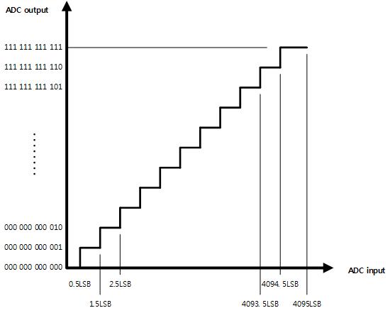
ADC Transform function description
SSP Interface Characteristics
| Symbol | Parameter | Conditions | Min | Max | Unit |
|---|---|---|---|---|---|
| fSCL | SSP clock frequency | Master mode | 20 | MHz | |
| Slave mode | 20 | MHz | |||
| tr_SCK | SSP clock rising and fall time | Capacitive load : C = 25pF | 8 | ns | |
| tSU_M | Data input setup time | Master mode | 5 | ns | |
| tSU_S | Slave mode | 6 | ns | ||
| tH_M | Data input hold time | Master mode | 5 | ns | |
| tH_S | Slave mode | 6 | ns | ||
| tV_M | Data output valid time | Master mode | 20 | ns | |
| tV_S | Slave mode | 5 | ns | ||
| tH_M | Data output hold time | Master mode | 13 | ||
| tH_S | Slave mode | 3 | |||
| DuCy | SSP slave input clock duty cycle | Slavemode | 45 | 55 | % |
Package Characteristics
Package dimension information
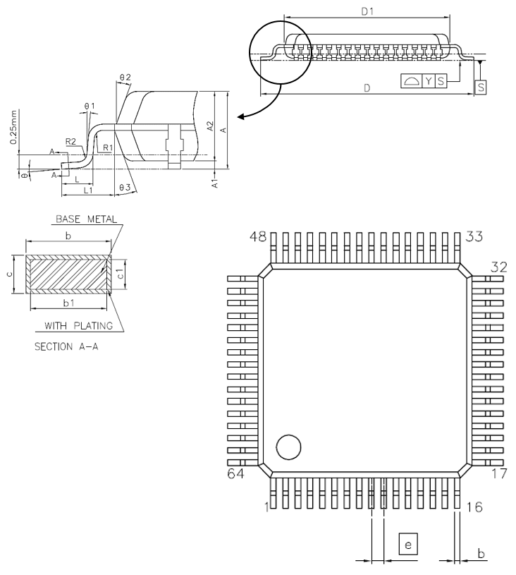
| Symbol | Dimention (MM) | Dimention (MIL) | ||||
|---|---|---|---|---|---|---|
| Min | Nom | Max | Min | Nom | Max | |
| A | 1.60 | 63.0 | ||||
| A1 | 0.05 | 0.10 | 0.15 | 2.0 | 3.9 | 5.9 |
| A2 | 1.35 | 1.40 | 1.45 | 53.1 | 55.1 | 57.1 |
| b | 0.13 | 0.18 | 0.23 | 5.1 | 7.1 | 9.1 |
| b1 | 0.13 | 0.16 | 0.19 | 5.1 | 6.3 | 7.5 |
| c | 0.09 | 0.20 | 3.5 | 7.9 | ||
| c1 | 0.09 | 0.16 | 3.5 | 6.3 | ||
| D | 8.85 | 9.00 | 9.15 | 348.4 | 354.3 | 360.2 |
| D1 | 6.90 | 7.00 | 7.10 | 271.7 | 275.6 | 279.5 |
 | 0.35 | 0.40 | 0.45 | 13.8 | 15.7 | 17.7 |
| L | 0.45 | 0.60 | 0.75 | 17.7 | 23.6 | 29.5 |
| L1 | 0.85 | 1.00 | 1.15 | 33.5 | 39.4 | 45.3 |
| R1 | 0.08 | 3.1 | ||||
| R2 | 0.08 | 0.20 | 3.1 | 7.9 | ||
| Y | 0.08 | 3.1 | ||||
| θ | 0° | 3.5° | 7° | 0° | 3.5° | 7° |
| θ1 | 0° | 0° | ||||
| θ2 | 11° | 12° | 13° | 11° | 12° | 13° |
| θ3 | 11° | 12° | 13° | 11° | 12° | 13° |
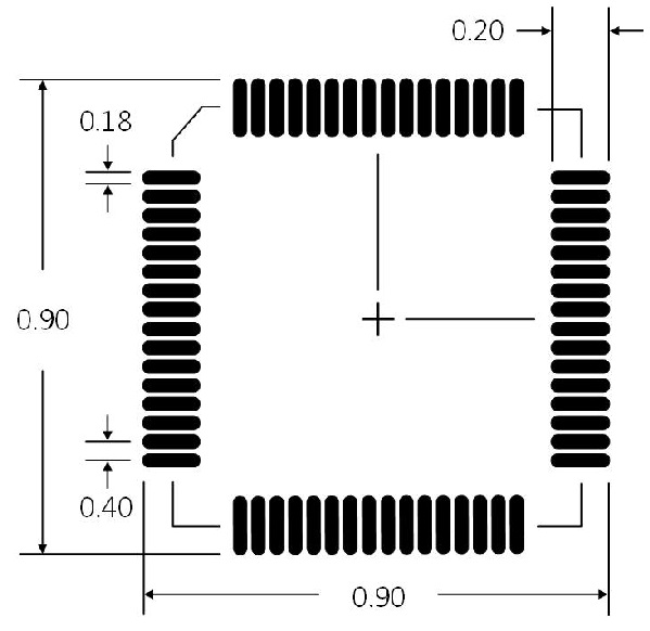
Package footprint information