WIZ750SR-100 Datasheet
Hardware Specification
Product Spec Table
| Category | Description | |
|---|---|---|
| MCU | ARM Cortex-M0 Core | W7500 48Mhz maximum frequency Internal 8Mhz RC Oscillator Flash: 128KB Large flexible-size SRAM buffer for various User Application - Min 16KB available if full 32KB socket buffer used - Max 48KB available if no socket buffer used ROM for boot code: 6 KB |
| MCU | Hardwired TCP/IP Core | 8 independent Sockets SRAM for socket: 32KB MII (Medium-Independent Interface) TCP/IP Protocols: TCP, UDP, ICMP, IPv4, ARP, IGMP, PPPoE |
| PHY | Transceiver | IP101GRI Single 10/100M Ethernet Transceiver |
| Serial | Interface | UART (LVTTL 3.3V) |
| Serial | Signal | TXD, RXD, RTS, CTS, DTR, DSR GND |
| Serial | Parameters | Parity: None, Odd, Even Data bits: 7, 8 bit Flow control: None, RTS / CTS, XON / XOFF |
| Serial | Speed | Up to 230Kbps |
| Dimension | 50mm x 30mm x 12mm (Include part size) | |
| Connector type | Mount Connector 2.00mm Pitch 1x12 Pin-header 2EA Not Mount Connector 2.00mm Pitch 1x12 Pin-header 1ea 2.54mm Pitch 1x6 Pin-header 1.27mm Pitch 1x5 Pin-header | |
| Input Voltage | DC 3.3V, 100mA under | |
| Temperature | -40℃ ~ 85℃ (Operation), -40℃ ~ 85℃ (Storage range) |
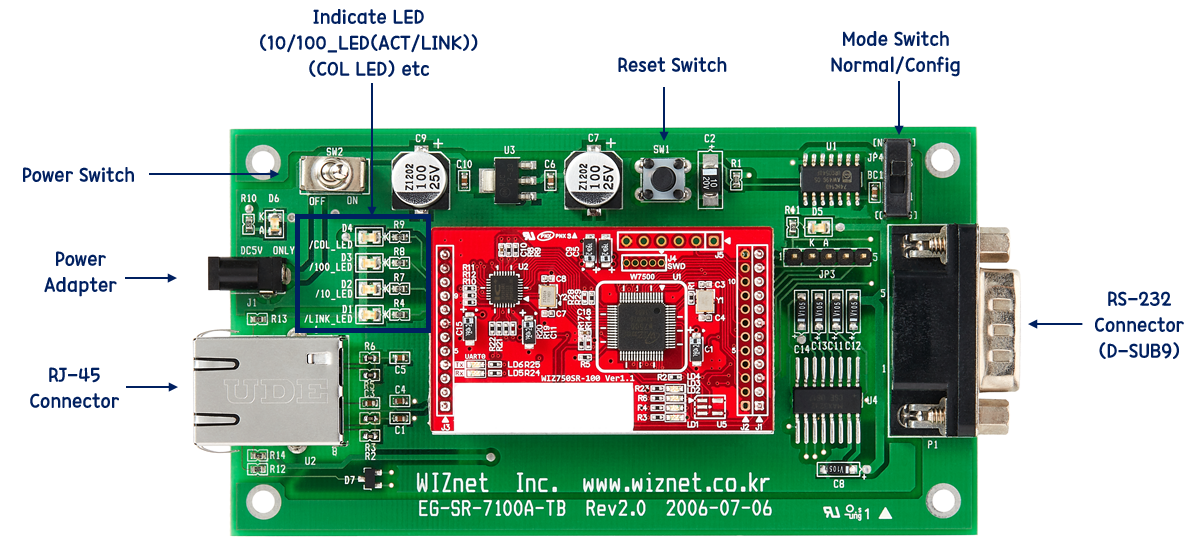
WIZ750SR-100 Callout
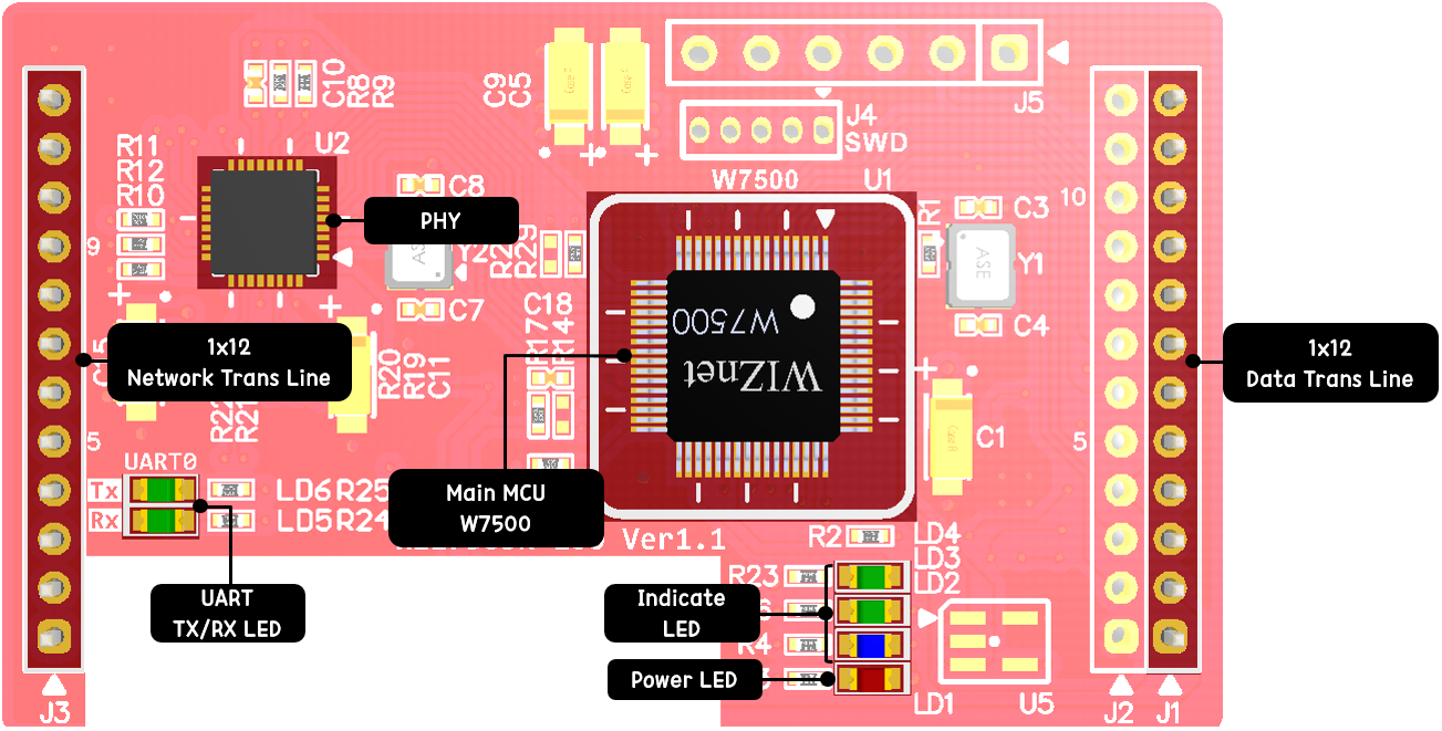 |
| TOP |
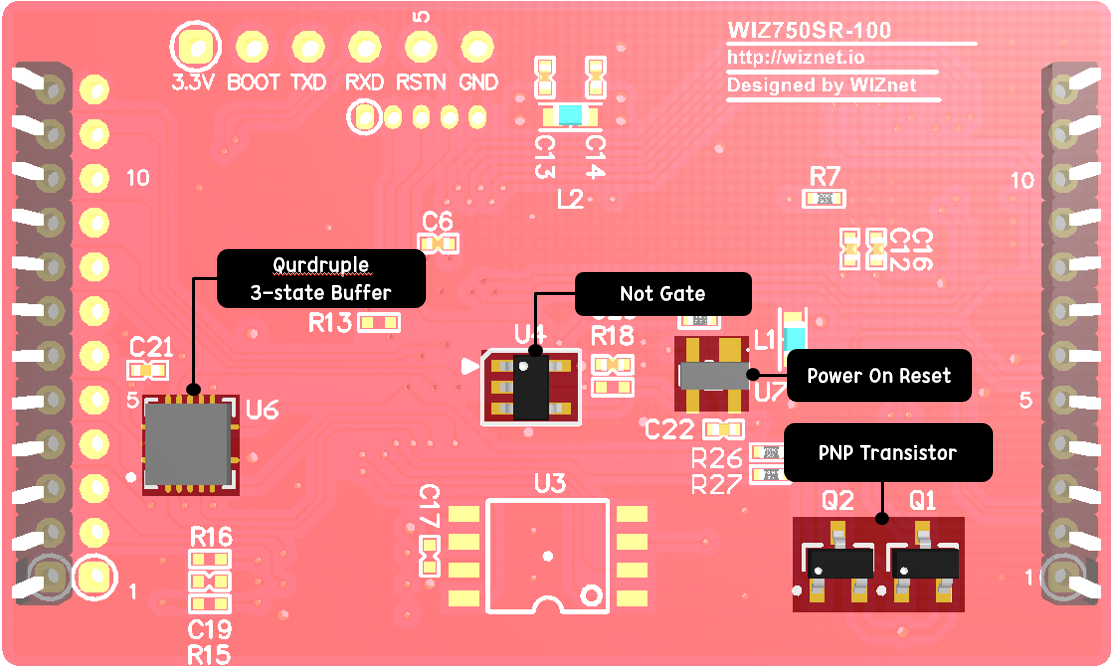 |
| BOTTOM |
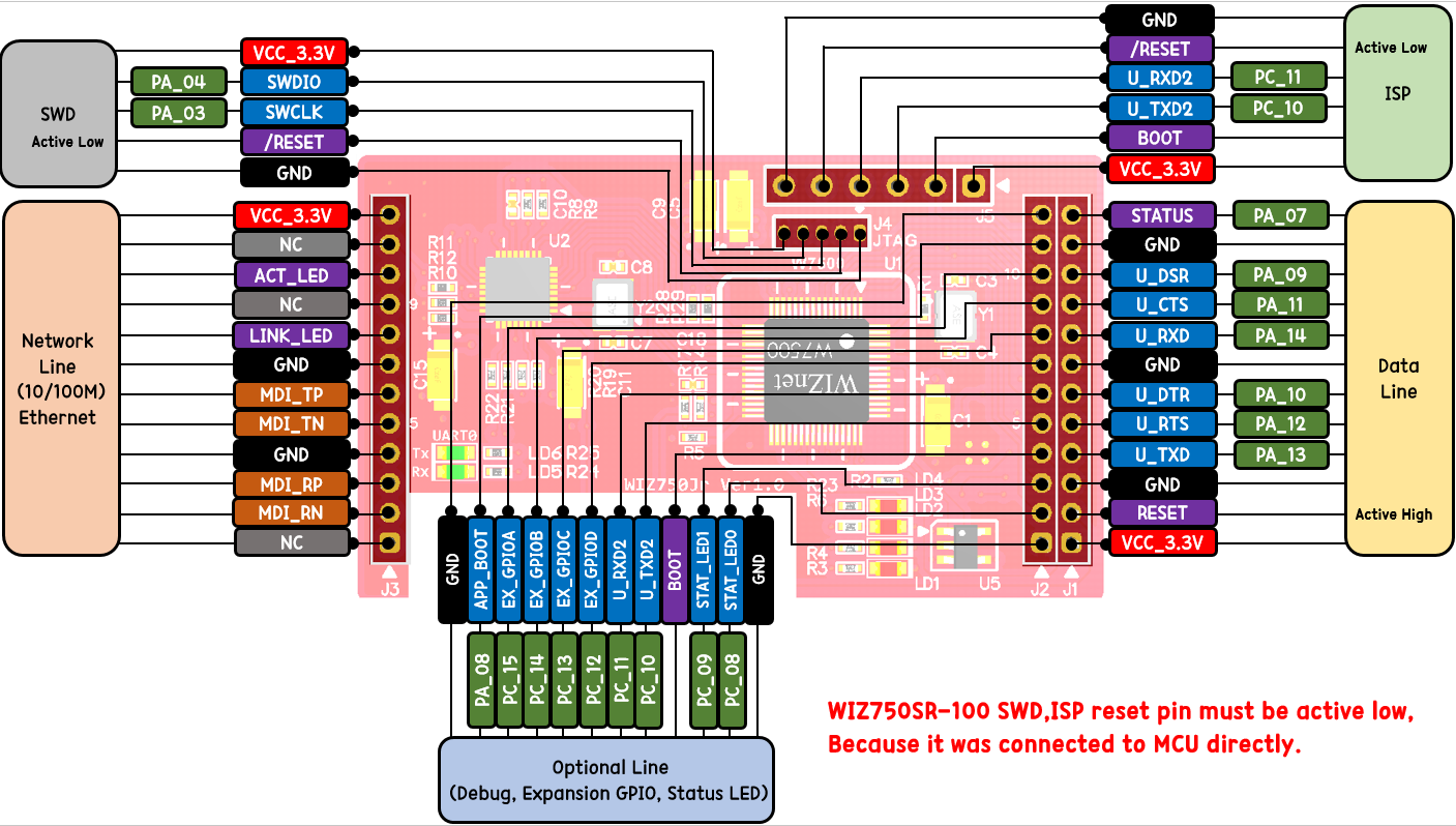
WIZ750SR-100 Pinout
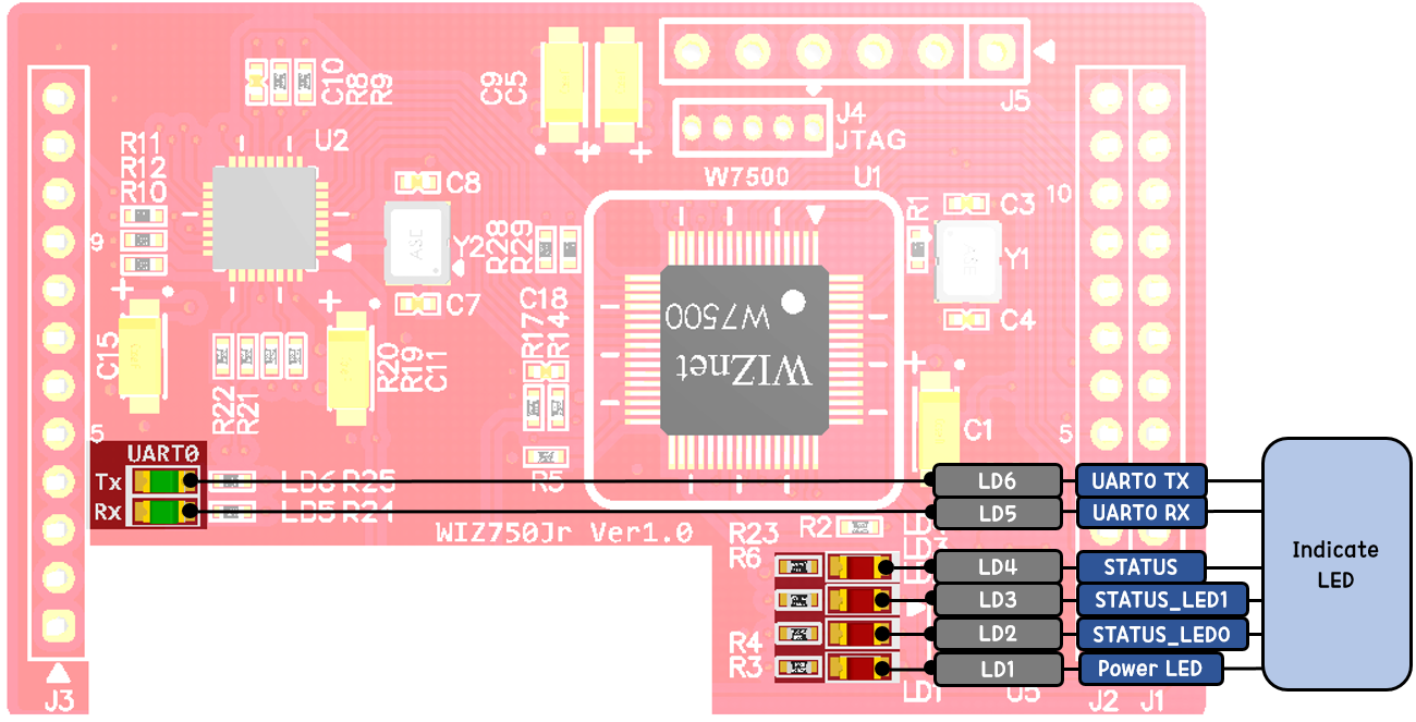
WIZ750SR-100 indicate
| Pin Number | Pin Name | Signal | Description |
|---|---|---|---|
| 1 | LD1 | Power LED | - |
| 2 | LD2 | Status_LED0 | PHY LINK check or initialize done |
| 3 | LD3 | Status_LED1 | TCP Connectoin |
| 4 | LD4 | STATUS | Trigger mode indicate TCP connection indicate |
| 5 | LD5 | UART0 RX | UART receiver indicate |
| 6 | LD6 | UART0 TX | UART Transceiver indicate |
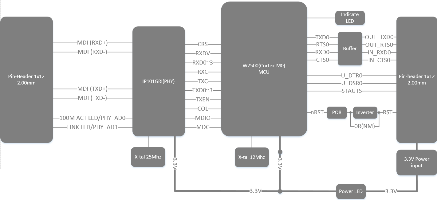
WIZ750SR-100 Block Diagram
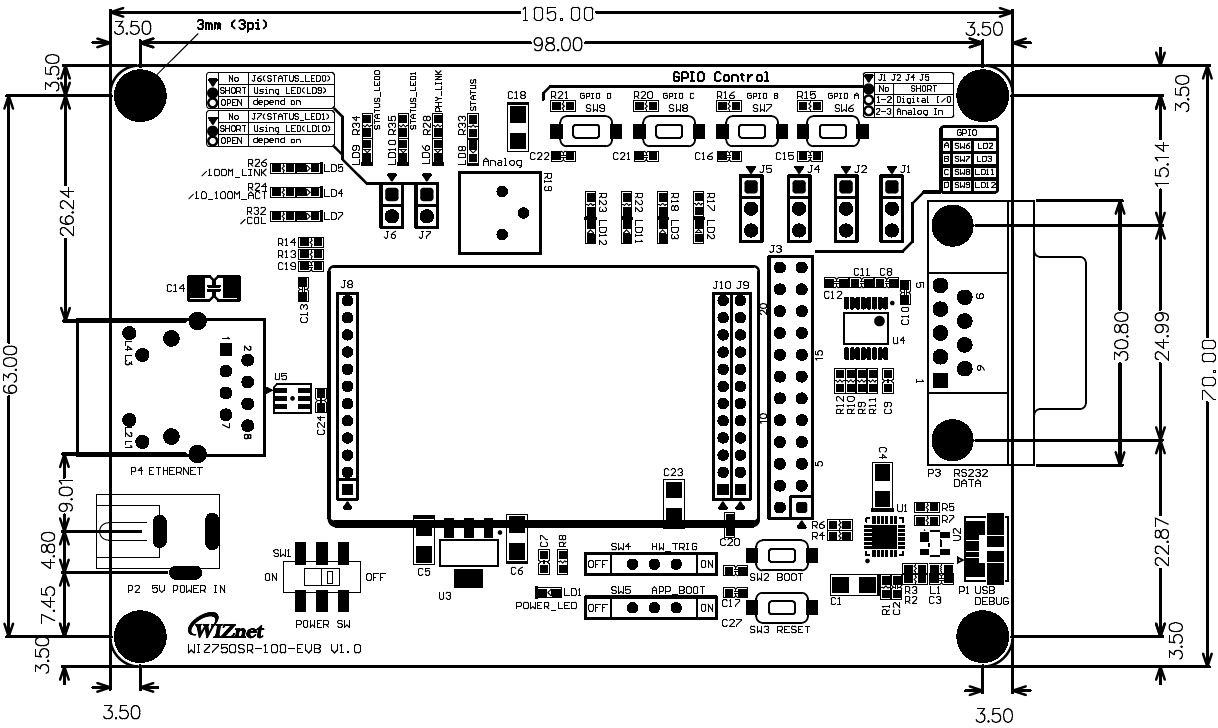
WIZ750SR-100-EVB
- WIZ750SR-100 Developer Board.
- USB to UART chip, CP2104.
- RESET Tact SW.
- BOOT0 Slide SW.
- H/W Trig Slide SW.
- Expansion GPIO TEST (Digital / Analog)
- Micro USB.
- WIZ750SR-100-EVB (RS-232)
- RS-232C Transceiver, D-SUB9-MALE.
Serial Interface
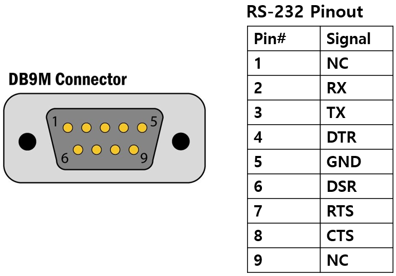
| Pin Number | Signal | Description |
|---|---|---|
| 1 | DCD | NC |
| 2 | RXD | Receive Data |
| 3 | TXD | Transmit Data |
| 4 | DTR | Data Terminal Ready |
| 5 | GND | System Ground(Signal Ground) |
| 6 | DSR | Data Set Ready |
| 7 | RTS | Request To Send |
| 8 | CTS | Clear To Send |
| 9 | RI | NC |
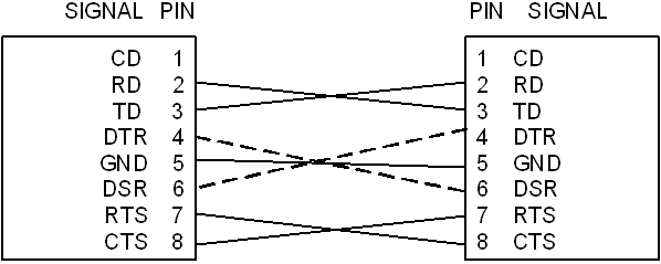
- RXD, TXD, GND: These are all you need if the device does not use hardware handshaking.
- RXD, TXD, GND, RTS, CTS: These are the signals used when serial device uses hardware handshaking.
- DTR, DSR: Not used
Schematic & Artwork
WIZ750SR-100
| H/W version | Type | Filetype | Download Link | Remarks |
|---|---|---|---|---|
| 1.0 | TTL | Altium | - | |
| ::: | ::: | - | ||
| 1.1 | TTL | Altium | - | |
| ::: | ::: | - |
WIZ750SR-EVB
| H/W version | Type | Filetype | Download Link | Remarks |
|---|---|---|---|---|
| 1.0 | RS232 | Altium | - | |
| ::: | ::: | - |
3D File
| H/W version | Type | Filetype | Download Link | Remarks |
|---|---|---|---|---|
| 1.1 | TTL | Altium | - |
Part list
WIZ750SR-100
| H/W version | Type | Filetype | Download Link | Remarks |
|---|---|---|---|---|
| 1.0 | TTL | Excel | ||
| ::: | ::: | |||
| 1.1 | TTL | Excel | ||
| ::: | ::: |
WIZ750SR-100-EVB
| H/W version | Type | Filetype | Download Link | Remarks |
|---|---|---|---|---|
| 1.0 | TTL | Excel | ||
| ::: | ::: |
Electrical Characteristics
Operating Conditions
| Symbol | Parameter | Pins | Min | Typ | Max | Unit |
|---|---|---|---|---|---|---|
| Vcc | Operating Voltage | 3.3V | 3.135 | 3.3 | 3.465 | V |
| Vss | Ground | ALL | 0 | 50 | mV | |
| fFCLK | Internal CPU clock frequency | ALL | 0 | - | 48 | MHz |
| Tstg | Storage Temperature (max) | ALL | -40 | 85 | ℃ | |
| TA | Ambient operating temperature | ALL | -40 | 85 | ℃ | |
| VIO | I/O Signal voltage (Tolerance) | ALL | Vss-0.3 | 3.3 | 5 | V |
| VIH | Input high voltage | ALL | 2.5 | V | ||
| VIL | Input low voltage | ALL | 0.6 | V | ||
| VOH | Output high voltage (High driving strength Current load = 6mA) (Low driving strength Current load = 3mA) | ALL | 2.83 | V | ||
| VOL | Output high voltage (High driving strength Current load = 6mA) (Low driving strength Current load = 3mA) | ALL | 0.32 | V |
Flash Memory
| Symbol | Parameter | Min | Unit |
|---|---|---|---|
| NEND | Sector Endurance | 10,000 | Cycles |
| TDR | Data Retention | 10 | Years |
EEPROM
| Symbol | Parameter | Min | Unit |
|---|---|---|---|
| NEND | Sector Endurance | 1M | Cycles |
| TDR | Data Retention | 200 | Years |
Connector Specification
1x12 Data Pin Connector (J1)
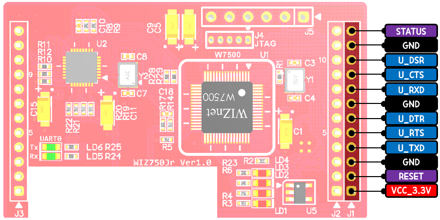
| Pin Number | Signal | Description |
|---|---|---|
| 1 | VCC | System Power input (3.3V) |
| 2 | RESET | System Reset signal (Active HIGH) |
| 3 | GND | System Ground |
| 4 | U_TXD0 | Transmit Data (TTL : 3.3V) |
| 5 | U_RTS0 | Request To Send (TTL : 3.3V) |
| 6 | U_DTR0 PHY LINK | Data Terminal Ready (TTL : 3.3V) PHY Link status check signal |
| 7 | GND | System Ground |
| 8 | U_RXD0 | Receive Data (TTL : 3.3V) |
| 9 | U_CTS0 | Clear To Send (TTL : 3.3V) |
| 10 | U_DSR0 TCP CON HW_TRIG | Data Set Ready (TTL : 3.3V) TCP Connection check signal |
| 11 | GND | System Ground |
| 12 | STATUS | TCP Connection & Trigger mode High: Not Connected Low: Connected |
| ::: | HW_TRIG | Hardware Trigger (Only Check once at booting) High & Floating: Normal mode Low: App boot mode |
- STATUS pin was changed HW_TRIG pin.
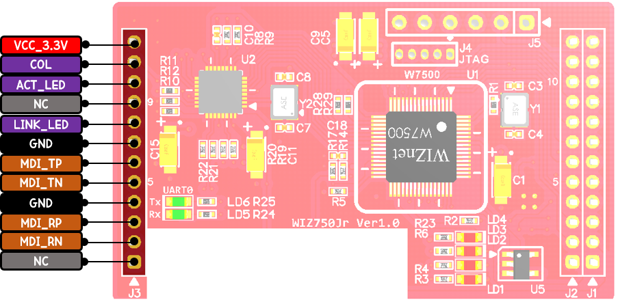
1x12 Network Line (J3)
WIZ750SR Rev1.0
WIZ750SR Rev1.1
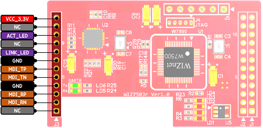
| Pin Number | Signal | Description |
|---|---|---|
| 1 | NC | Not Connect |
| 2 | MDI_RN | 10/100M MDIO Receiver Differential Signal (N signal) |
| 3 | MDI_RP | 10/100M MDIO Receiver Differential Signal (P signal) |
| 4 | GND | System Ground |
| 5 | MDI_TN | 10/100M MDIO Transceiver Differential Signal (N signal) |
| 6 | MDI_TP | 10/100M MDIO Transceiver Differential Signal (P signal) |
| 7 | GND | System Ground |
| 8 | Link LED | High: Link down Low: Link up (When the PHY is physically connected, the LINK LED lights up.) |
| 9 | NC | Not Connect |
| 10 | ACT LED | Blink: 100M ACT (ACT LED blinks when data is transmitted/received between PHYs.) |
| 11 | NC | Not Connect (This pin connected to COL pin in Rev1.0. this pin outputs a high-status signal it means a collision is detected. Processed to NC in Rev1.1.) |
| 12 | VCC | System Power input (3.3V) |
1x12 Expansion GPIO & APP BOOT & Debug(ISP) Port (J2)
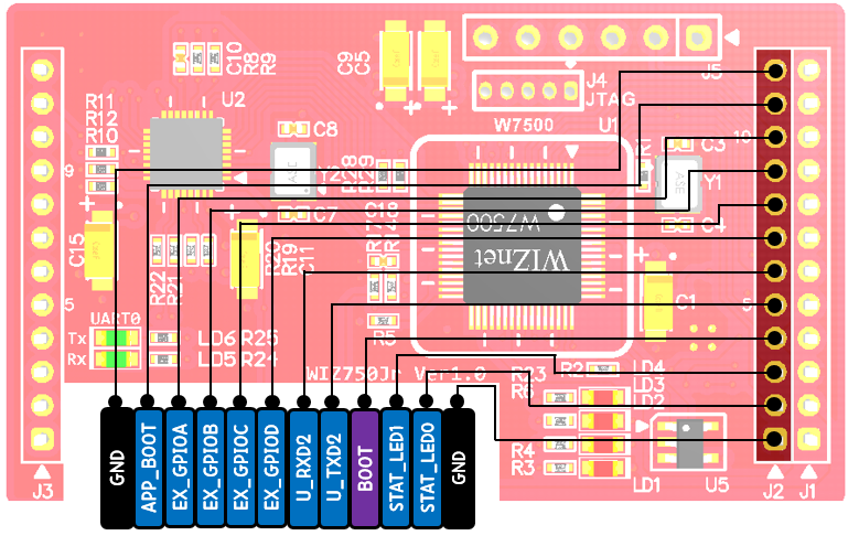
| Pin Number | Signal | Description |
|---|---|---|
| 1 | GND | System Ground |
| 2 | Status LED0 | User's depend on pin(LED) |
| 3 | Status LED1 | User's depend on pin(LED) |
| 4 | BOOT | BOOT SW |
| 5 | U_TXD2 | Simple UART2(Debug port) ISP mode firmware downloader port |
| 6 | U_RXD2 | Simple UART2(Debug port) ISP mode firmware downloader port |
| 7 | Expansion GPIOD | Expansion User's depend on GPIO port |
| 8 | Expansion GPIOC | ::: |
| 9 | Expansion GPIOB | ::: |
| 10 | Expansion GPIOA | ::: |
| 11 | APP BOOT | Application Jump at BOOT mode |
| 12 | GND | System Ground |
1x5 SWD
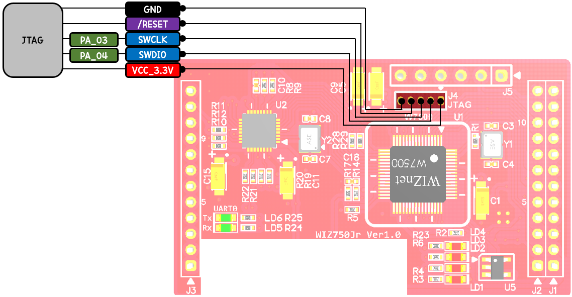
| Pin Number | Signal | Description |
|---|---|---|
| 1 | VCC | System Power input (3.3V) |
| 2 | SWDIO | SWD(JTAG) Data I/O pin |
| 3 | SWCLK | SWD(JTAG) Clock pin |
| 4 | nRESET | System Reset signal (Active Low)[1] |
| 5 | GND | System Ground |
Caution) WIZ750SR-100 SWD reset pin must be active low, because it was connected to MCU directly.
1x6 ISP
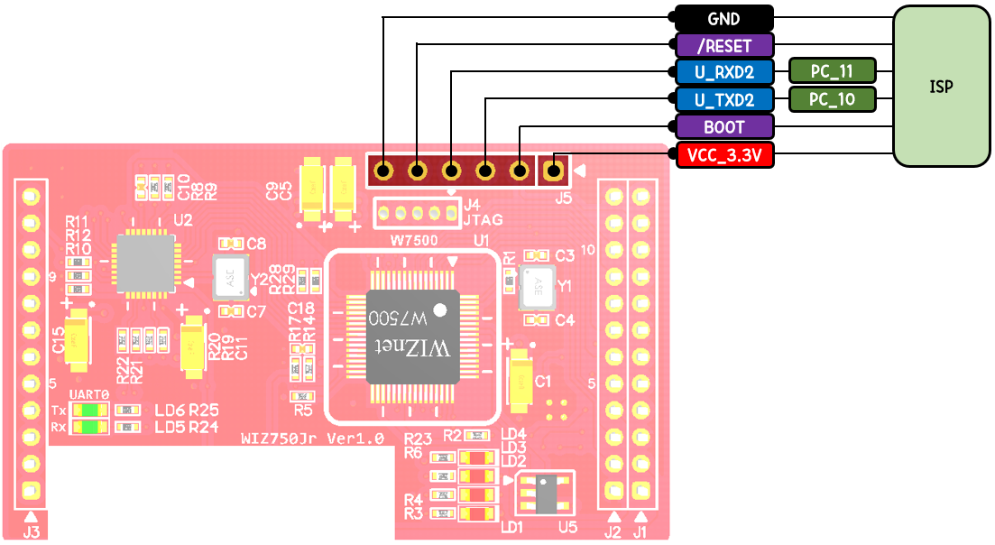
| Pin Number | Signal | Description |
|---|---|---|
| 1 | VCC | System Power input (3.3V) |
| 2 | BOOT | BOOT SW |
| 3 | U_TXD2 | Simple UART2(Debug port) ISP mode firmware downloader port |
| 4 | U_RXD2 | Simple UART2(Debug port) ISP mode firmware downloader port |
| 5 | nRESET | System Reset signal (Active Low)1 |
| 6 | GND | System Ground |
This pin connect to MCU reset pin directly↩︎
Caution) WIZ750SR-100 ISP reset pin must be active low, because it was connected to MCU directly.
RJ-45 Connector (BS-RB10005)
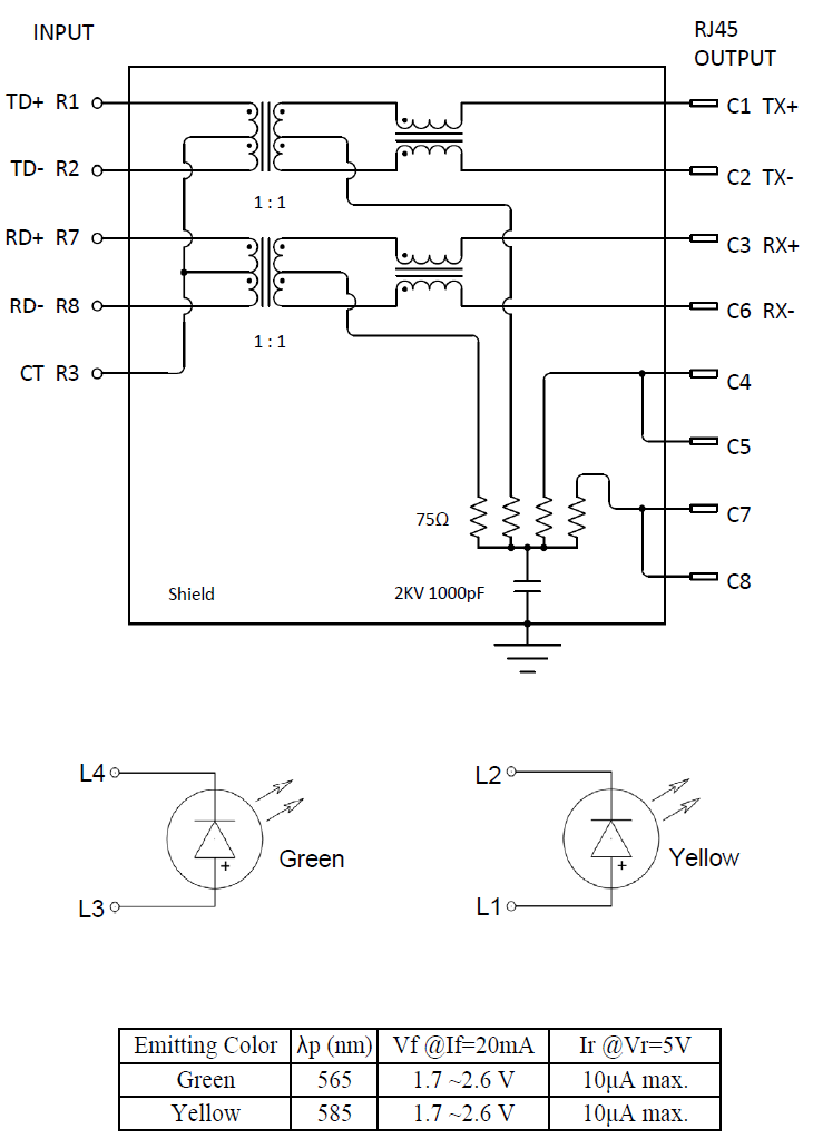
| Pin Number | Pin | Signal |
|---|---|---|
| 1 | R1 | TX+ |
| 2 | R2 | TX- |
| 3 | R3 | TCT/RCT(Center tap) |
| 4 | R7 | RX+ |
| 5 | R8 | RX- |
| 6 | L1+(Active LED) | Anode |
| 7 | L2- (Active LED) | Cathode |
| 8 | L3+(LINK LED) | Anode |
| 9 | L4- (LINK LED) | Cathode |
Dimension
- WIZ750SR-100 Rev1.0 Dimension :
- 50mm x 30mm ( PCB board size )
- 50mm x 30mm x 12mm ( Included part size )
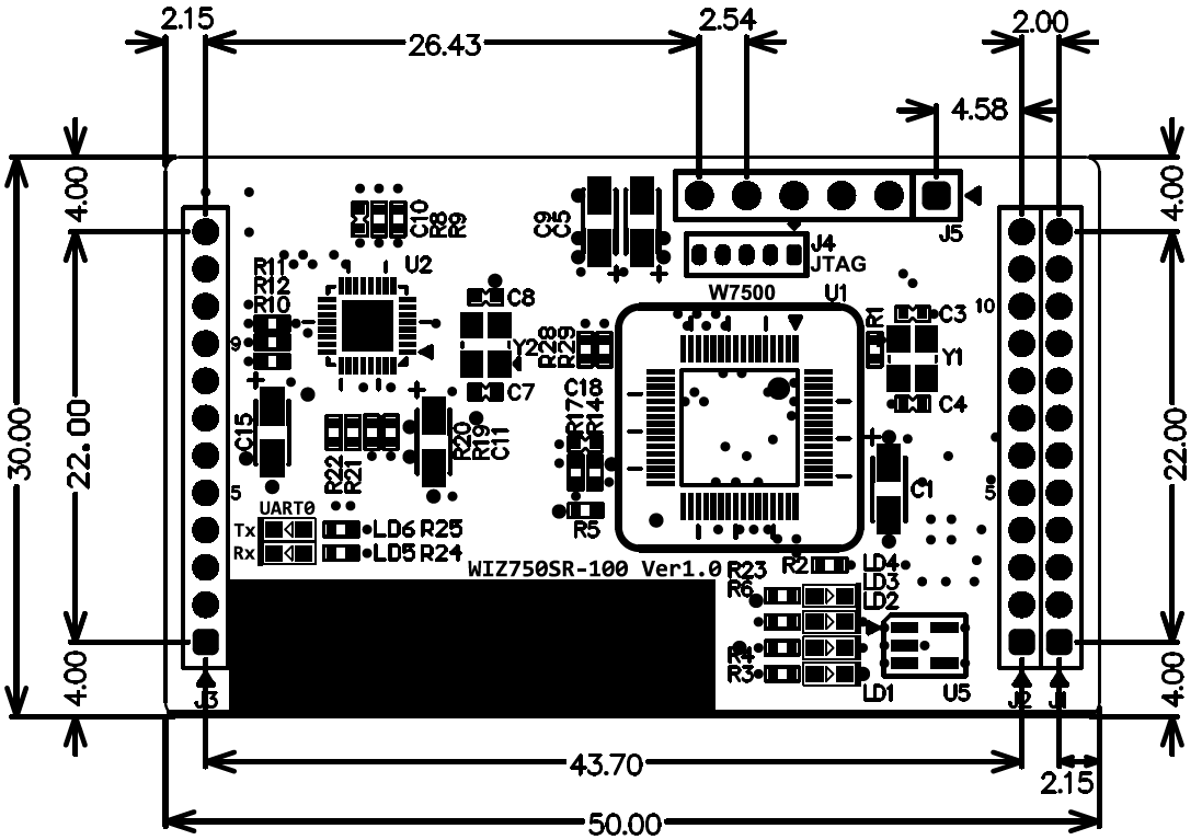
- WIZ750SR-100-EVB Rev1.0 Dimension :
- 105mm x 70mm ( PCB board size )
- 105mm x 70mm x 18mm ( Included part size )
[1] This pin connect to MCU reset pin directly