WIZSPE-T1L Datasheet
Hardware Specification
Product Spec Table
| Category | Description | |
|---|---|---|
| MCU | ARM Cortex-M0 Core | W7500 48Mhz maximum frequency Internal 8Mhz RC Oscillator Flash: 128KB Large flexible-size SRAM buffer for various User Application - Min 16KB available if full 32KB socket buffer used - Max 48KB available if no socket buffer used ROM for boot code: 6 KB |
| Hardwired TCP/IP Core | 8 independent Sockets SRAM for socket: 32KB MII (Medium-Independent Interface) TCP/IP Protocols: TCP, UDP, ICMP, IPv4, ARP, IGMP, PPPoE | |
| PHY | Transceiver | YT8111 Dual Robust 10Base-T1L Ethernet Transceiver |
| Serial | Signal | TXD, RXD, RTS, CTS, GND |
| Parameters | Parity: None, Odd, Even Data bits: 7, 8 bit Flow control: None, RTS / CTS, XON / XOFF | |
| Speed | Up to 230Kbps | |
| Dimension | TBD | |
| Connector type | TBD | |
| Input Voltage | TBD | |
| Temperature | TBD |
WIZSPE-T1L Callout
TBD (3D image)
WIZSPE-T1L Pinout
TBD (3D image)
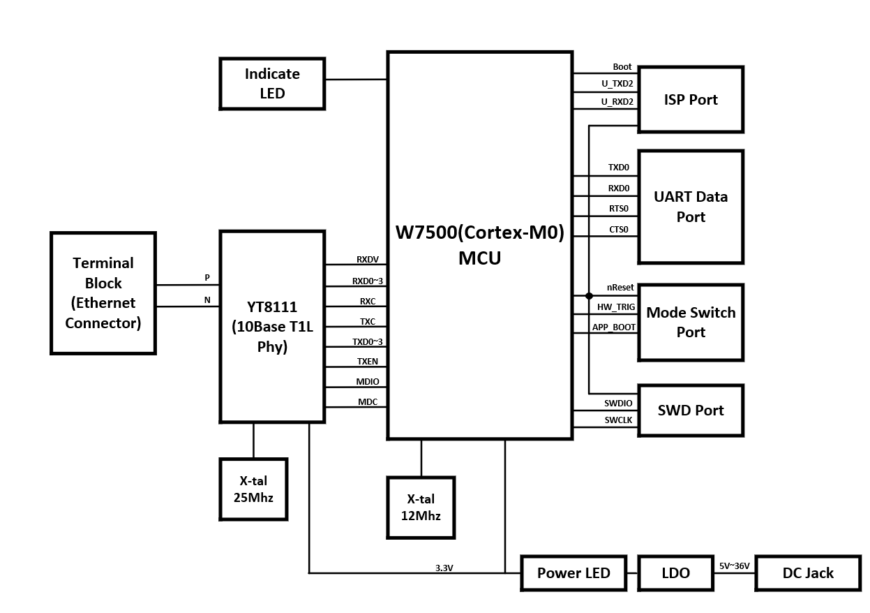
WIZSPE-T1L Block Diagram
Schematic & Artwork
WIZSPE-T1L
TBD
3D File
TBD
Part list
WIZSPE-T1L
TBD
Electrical Characteristics
Operating Conditions
TBD
Connector Specification
BOOT Pin (J7, J8)
| Parts | Pin Number | Signal | Description |
|---|---|---|---|
| J7 | 1 | APP BOOT | Application Jump at BOOT mode |
| ::: | 2 | GND | System Ground |
| Parts | Pin Number | Signal | Description |
|---|---|---|---|
| J8 | 1 | BOOT | System Ground |
| ::: | 2 | VCC | System Power (3.3V) |
SWD(JTAG) Pin (J10)
| Parts | Pin Number | Signal | Description |
|---|---|---|---|
| J10 | 1 | VCC | System Power (3.3V) |
| ::: | 2 | SWDIO | SWD(JTAG) Data I/O pin |
| ::: | 3 | SWCLK | SWD(JTAG) Clock pin |
| ::: | 4 | nRESET | System Reset signal (Active Low) |
| ::: | 5 | GND | System Ground |
ISP Port (J6)
| Parts | Pin Number | Signal | Description |
|---|---|---|---|
| J6 | 1 | VCC | System Power (3.3V) |
| ::: | 2 | BOOT | Go to Boot mode |
| ::: | 3 | UART2 TX | ISP Serial TX |
| ::: | 4 | UART2 RX | ISP Serial RX |
| ::: | 5 | nRESET | System Reset signal (Active Low) |
| ::: | 6 | GND | System Ground |
Serial Port (J11)
| Parts | Pin Number | Signal | Description |
|---|---|---|---|
| J11 | 1 | nRESET | System Reset signal (Active Low) |
| ::: | 2 | VCC | System Power (3.3V) |
| ::: | 3 | UART0 RX | Data Serial RX |
| ::: | 4 | VCC | System Power (3.3V) |
| ::: | 5 | UART0 CTS | Data Serial CTS |
| ::: | 6 | ::: | ::: |
| ::: | 7 | UART0 TX | Data Serial TX |
| ::: | 8 | HW_TRIG/UART0 DSR/ TCP | HW Trigger/ Data Serial DSR / TCP Status |
| ::: | 9 | UART0 RTS | Data Serial RTS |
| ::: | 10 | UART0 DTR/PHY LINK | Data Serial DTR / Phy link |
| ::: | 11 | GND | System Ground |
| ::: | 12 | GND | System Ground |
SPE Terminal Block (J2)
| Parts | Pin Number | Signal | Description |
|---|---|---|---|
| J2 | 1 | P | Positive (+) line of the SPE differential pair |
| ::: | 2 | N | Negative (–) line of the SPE differential pair |
| ::: | 3 | Earth | Earth Ground |