WIZ750SR-T1L Datasheet
Hardware Specification
Product Spec Table
| Category | Description | |
|---|---|---|
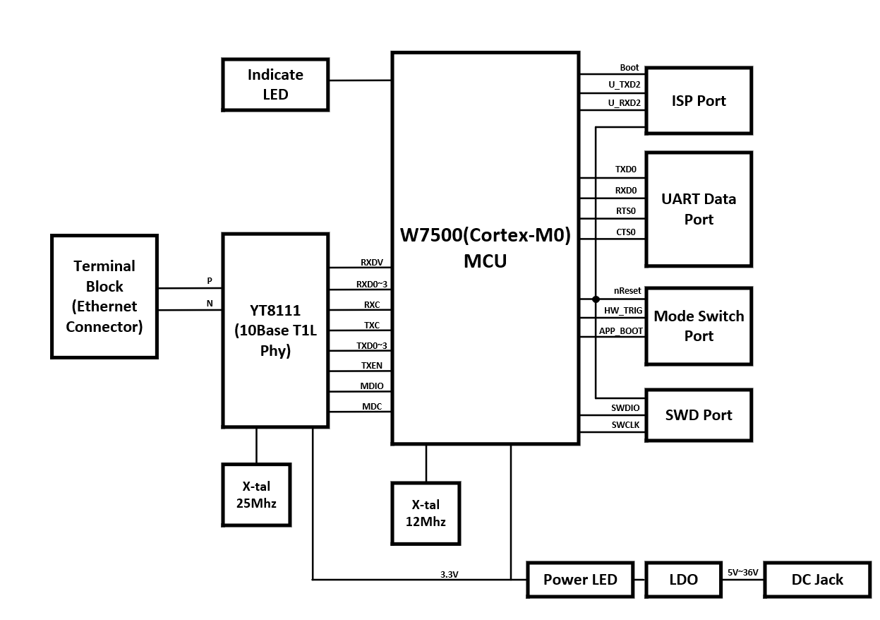
| MCU | ARM Cortex-M0 Core | W7500 48Mhz maximum frequency Internal 8Mhz RC Oscillator Flash: 128KB Large flexible-size SRAM buffer for various User Application - Min 16KB available if full 32KB socket buffer used - Max 48KB available if no socket buffer used ROM for boot code: 6 KB |
| Hardwired TCP/IP Core | 8 independent Sockets SRAM for socket: 32KB MII (Medium-Independent Interface) TCP/IP Protocols: TCP, UDP, ICMP, IPv4, ARP, IGMP, PPPoE | |
| PHY | Transceiver | 10Base-T1L Ethernet PHY |
| Serial | Signal | TXD, RXD, RTS, CTS, GND |
| Parameters | Parity: None, Odd, Even Data bits: 7, 8 bit Flow control: None, RTS / CTS, XON / XOFF | |
| Speed | Up to 230Kbps | |
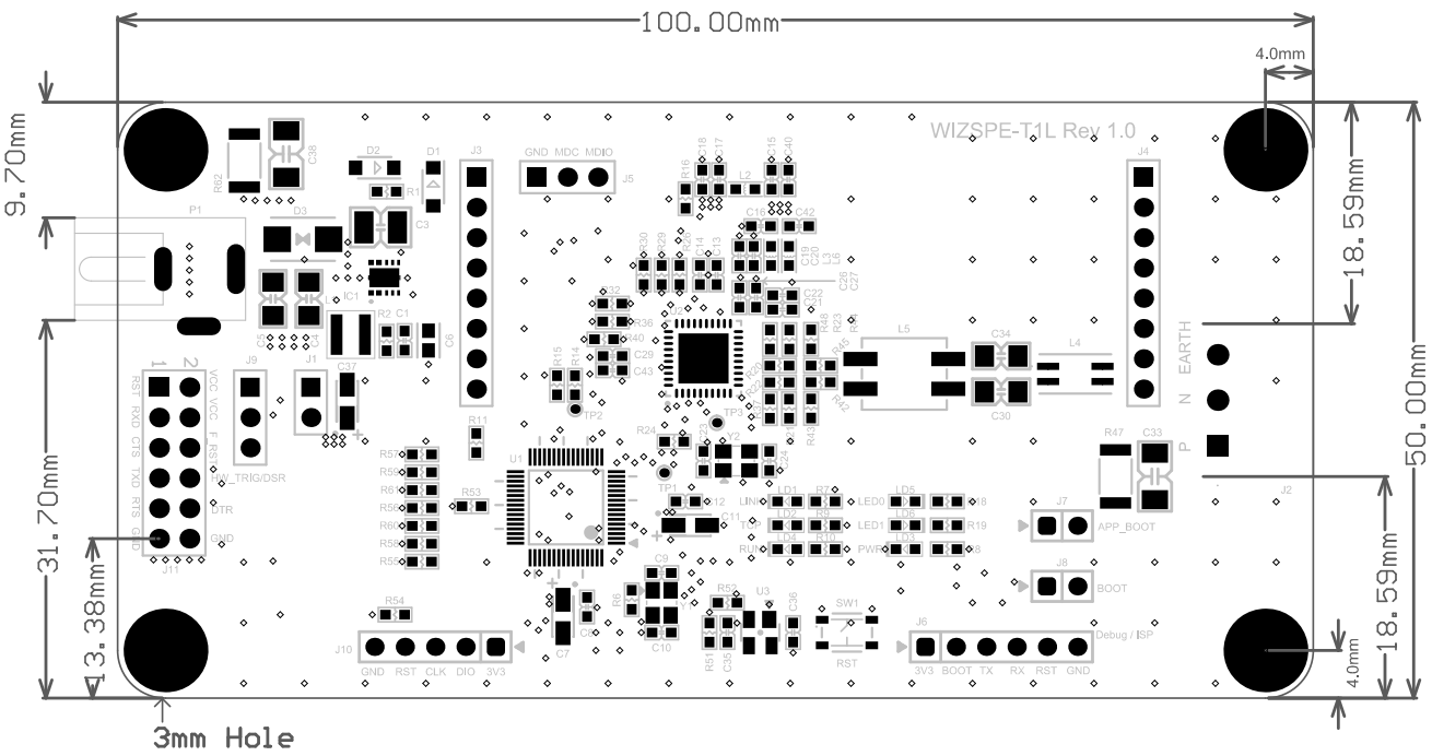
| Dimension | 100mm x 50mm x 1.6mm | |
| Connector type | 2.54mm Pitch 6x2 Pin-header(Data Line), 3.81mm Pitch 3pin Pluggable terminal Block(Jack) | |
| Input Voltage | Power - 5.0V ~ 36.0V Data Line - 3.3V LVTTL | |
| Temperature | -40℃ ~ 85℃ (Operation, Storage range) |
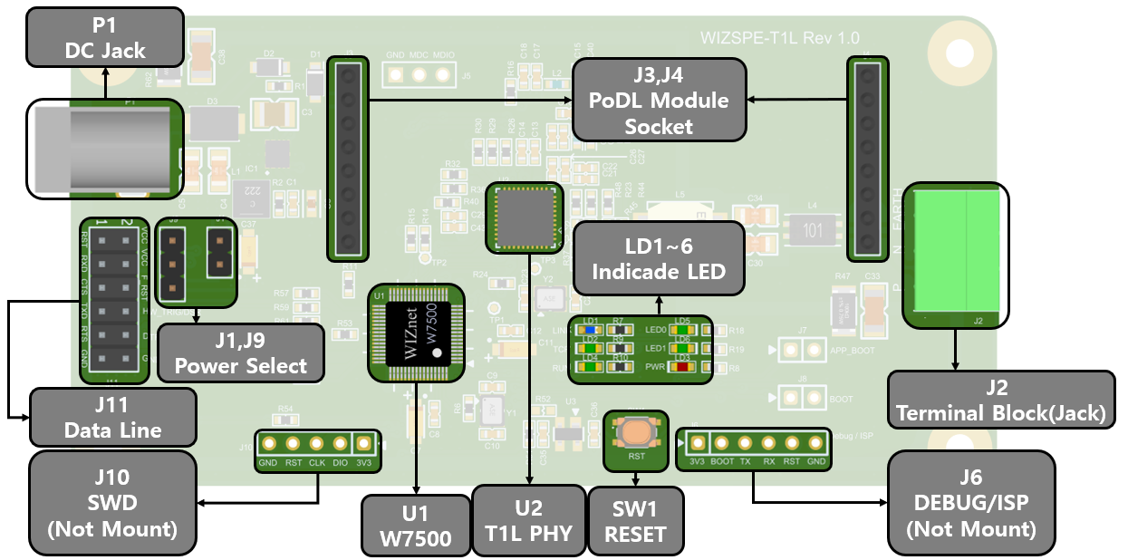
WIZ750SR-T1L Callout
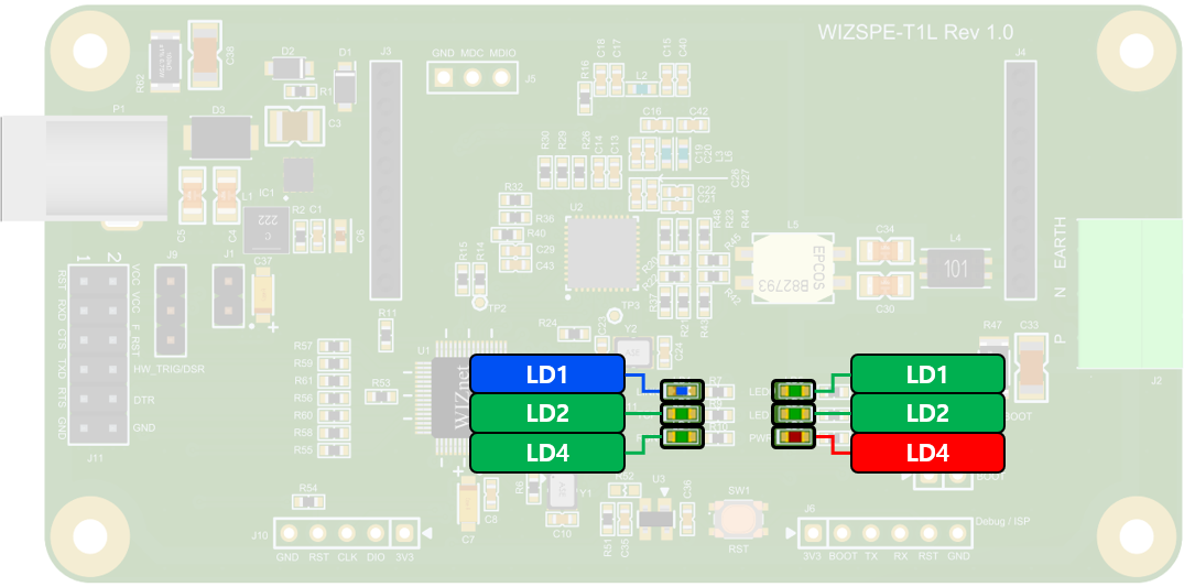
WIZ750SR-T1L Indicator
| Parts | Description |
|---|---|
| LD1 | Link LED |
| LD2 | TCP Connection LED |
| LD3 | Power LED |
| LD4 | Application Running LED |
| LD5 | User Config LED |
| LD6 | User Config LED |
WIZ750SR-T1L Block Diagram
Schematic & Artwork
| H/W version | Type | Filetype | Download Link | Remarks |
|---|---|---|---|---|
| 1.0 | - | Altium | - | |
| ::: | ::: | - |
3D File
| H/W version | Type | Filetype | Download Link | Remarks |
|---|---|---|---|---|
| 1.0 | - | STEP | - |
Part list
| H/W version | Type | Filetype | Download Link | Remarks |
|---|---|---|---|---|
| 1.0 | - | Excel | - | |
| ::: | ::: | - |
Electrical Characteristics
| Symbol | Parameter | Pins | Min | Typ | Max | Unit |
|---|---|---|---|---|---|---|
| Power | Power Source | DC JACK | 5.0 | - | 36 | V |
| VCC | W7500 Operating Voltage | W7500 VCC | 3.135 | 3.3 | 3.465 | V |
| Vss | Ground | ALL | 0 | 50 | mV | |
| fFCLK | Internal CPU clock frequency | W7500 | 0 | - | 48 | MHz |
| VIO | I/O Signal voltage (Tolerance) | W7500 IO | Vss-0.3 | 3.3 | 3.6 | V |
Operating Conditions
| Symbol | Parameter | Pins | Min | Typ | Max | Unit |
|---|---|---|---|---|---|---|
| Tstg | Storage Temperature (max) | ALL | -40 | 85 | ℃ | |
| TA | Ambient operating temperature | ALL | -40 | 85 | ℃ |
Connector Specification
Power Source Select Pin (J1, J9)
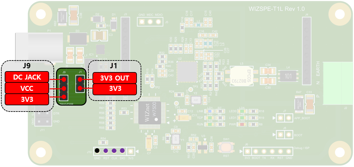
| Parts | Pin Number | Signal | Description |
|---|---|---|---|
| J1 | 1 | 3V3_OUT | This pin is connect with IC1(Step Down Convertor) output |
| ::: | 2 | 3V3 | System Power (3.3V) |
| Parts | Pin Number | Signal | Description |
|---|---|---|---|
| J9 | 1 | DC_JACK | This pin is connect with DC_Jack |
| ::: | 2 | VCC | This pin is connect with J11_VCC pin |
| ::: | 3 | 3V3 | System Power (3.3V) |
Set J1 and J9 according to the way you want to supply power to the module.
| Power Source | Input Voltage | J1 Set | J9 Set |
|---|---|---|---|
| DC Jack | 5 - 36 VDC | 1, 2 pin Short | NC |
| J11_VCC pin | 3.3 VDC | NC | 2, 3 pin Short |
| J11_VCC pin | 5 - 36 VDC | 1, 2 pin Short | 1, 2 pin Short |
APP/BOOT Pin (J7, J8)
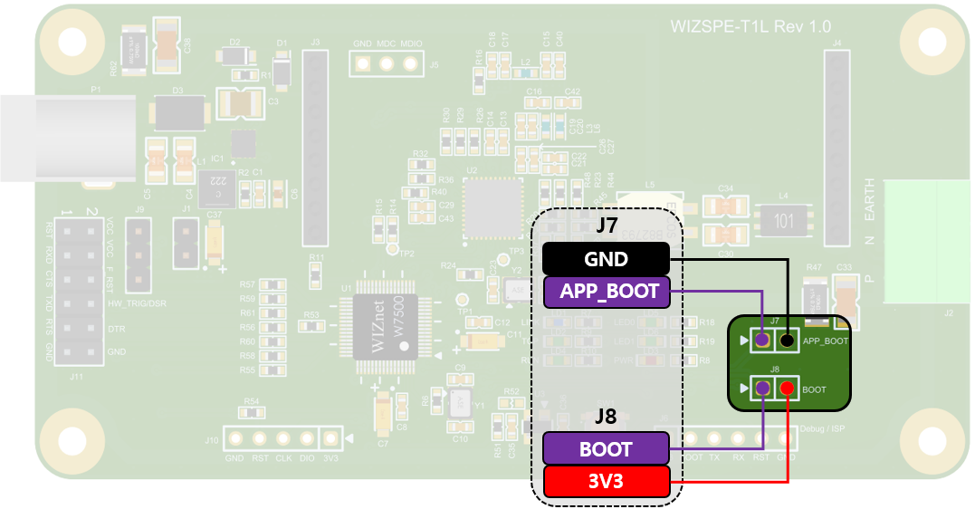
| Parts | Pin Number | Signal | Description |
|---|---|---|---|
| J7 | 1 | APP BOOT | Application Jump at BOOT mode (Active Low) When this pin is held Low and reset, the system runs only the Boot code and does not jump to the App code, unlike normal operation. This mode is used for debugging and forced uploading to the App area. |
| ::: | 2 | GND | System Ground |
| Parts | Pin Number | Signal | Description |
|---|---|---|---|
| J8 | 1 | BOOT | Boot mode Pin (Active High) |
| ::: | 2 | VCC | System Power (3.3V) |
For pin J7, the Boot mode refers to the code area’s Boot process. For pin J8, the Boot mode refers to the W7500’s native Boot mode, which allows ISP (In-System Programming) functionality.
SWD(JTAG) Pin (J10)
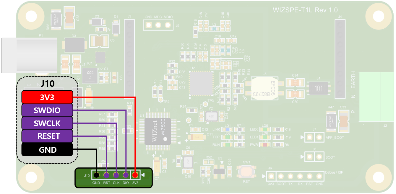
| Parts | Pin Number | Signal | Description |
|---|---|---|---|
| J10 | 1 | VCC | System Power (3.3V) |
| ::: | 2 | SWDIO | SWD(JTAG) Data I/O pin |
| ::: | 3 | SWCLK | SWD(JTAG) Clock pin |
| ::: | 4 | nRESET | System Reset signal (Active Low) |
| ::: | 5 | GND | System Ground |
ISP/DEBUG Port (J6)
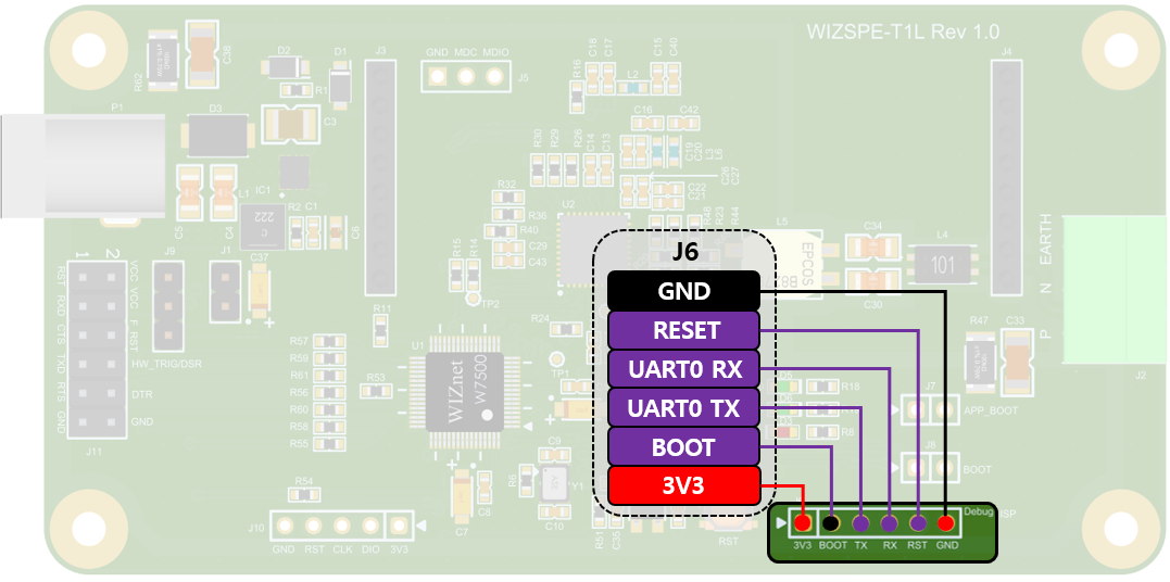
| Parts | Pin Number | Signal | Description |
|---|---|---|---|
| J6 | 1 | VCC | System Power (3.3V) |
| ::: | 2 | BOOT | Boot mode Pin (Active High) |
| ::: | 3 | UART2 TX | ISP Serial TX |
| ::: | 4 | UART2 RX | ISP Serial RX |
| ::: | 5 | nRESET | System Reset signal (Active Low) |
| ::: | 6 | GND | System Ground |
Serial Port (J11)
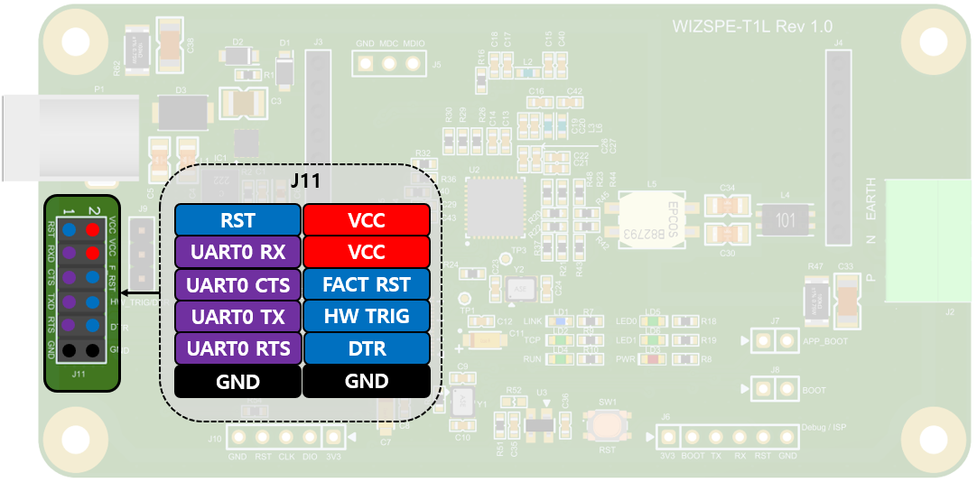
| Parts | Pin Number | Signal | Description |
|---|---|---|---|
| J11 | 1 | nRESET | System Reset signal (Active Low) |
| ::: | 2 | VCC | System Power (3.3V) |
| ::: | 3 | UART0 RX | Data Serial RX |
| ::: | 4 | VCC | System Power (3.3V) |
| ::: | 5 | UART0 CTS | Data Serial CTS |
| ::: | 6 | FACTORY RESET | Factory Reset signal (Active 5.0s Low) |
| ::: | 7 | UART0 TX | Data Serial TX |
| ::: | 8 | HW_TRIG/UART0 DSR/ TCP | HW Trigger/ Data Serial DSR / TCP Status |
| ::: | 9 | UART0 RTS | Data Serial RTS |
| ::: | 10 | UART0 DTR/PHY LINK | Data Serial DTR / Phy link |
| ::: | 11 | GND | System Ground |
| ::: | 12 | GND | System Ground |
SPE Terminal Block (J2)
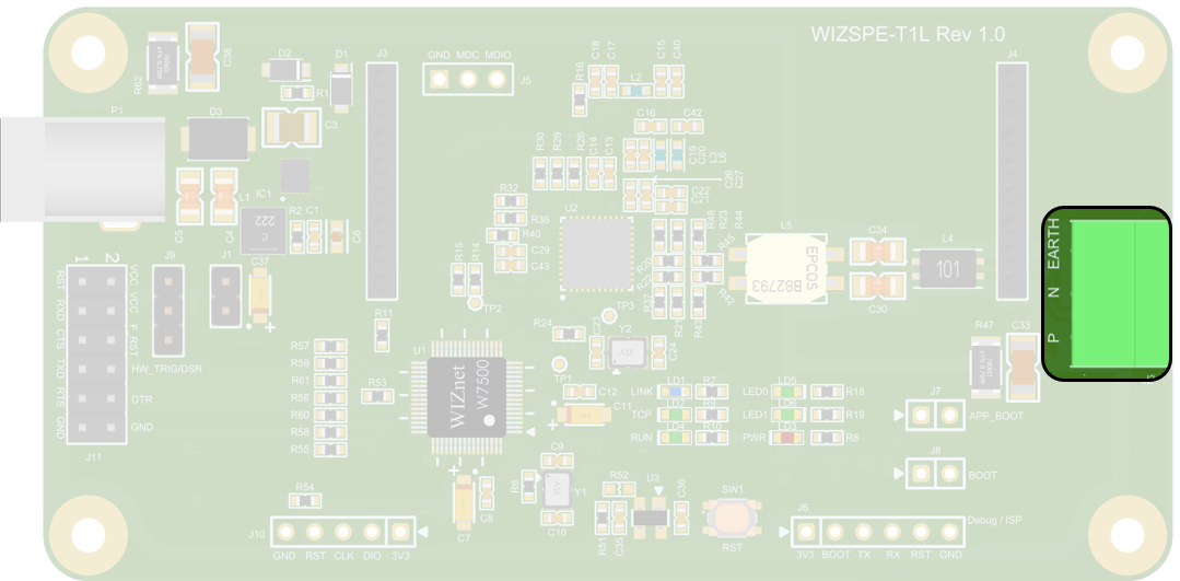
| Parts | Pin Number | Signal | Description |
|---|---|---|---|
| J2 | 1 | P | Positive (+) line of the SPE differential pair |
| ::: | 2 | N | Negative (–) line of the SPE differential pair |
| ::: | 3 | Earth | Earth Ground |
Dimension