Datasheet
Hardware Specification
Product Spec Table
| Category | Description | |
|---|---|---|
| MCU | ARM Cortex-M0 Core | W7500 1. 48Mhz maximum frequency 2. Internal 8Mhz RC Oscillator 3. Flash: 128KB 4. Large flexible-size SRAM buffer for various User Application - Min 16KB available if full 32KB socket buffer used - Max 48KB available if no socket buffer used 5. ROM for boot code: 6 KB |
| Hardwired TCP/IP Core | 1. 8 independent Sockets 2. SRAM for socket: 32KB 3. MII (Medium-Independent Interface) 4. TCP/IP Protocols: TCP, UDP, ICMP, IPv4, ARP, IGMP, PPPoE | |
| PHY | Transceiver | IP101GRI 1. Single 10/100M Ethernet Transceiver |
| Serial | Interface | W7500S2E-R1: TTL |
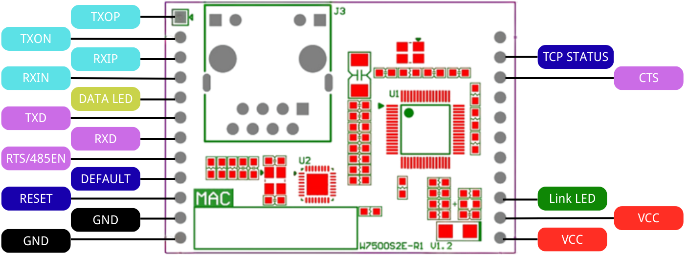
| Signal | TXD, RXD, RTS, CTS, GND | |
| Parameters | 1. Parity: None, Odd, Even 2. Data bits: 7, 8 bit 3. Flow control: None, RTS / CTS | |
| Baud Rate Speed | 300 bps to 460,800 bps | |
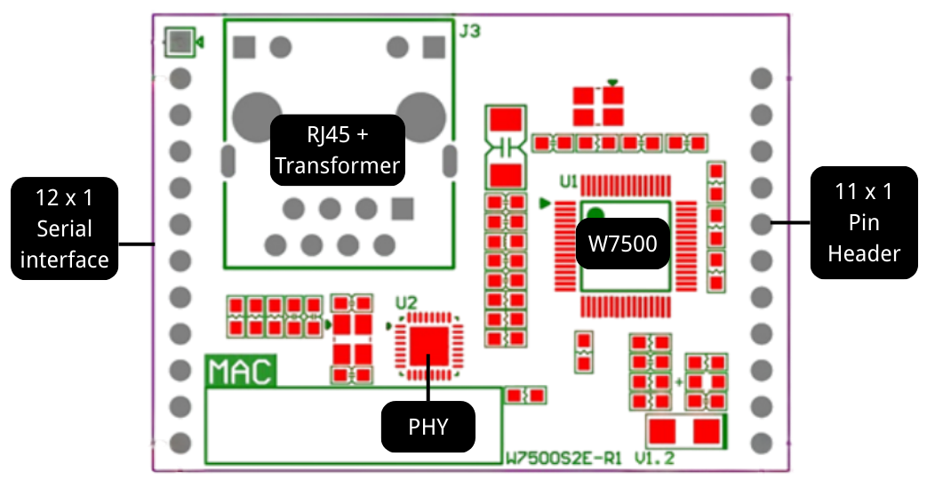
| Dimension | L x W x H | W7500S2E-R1: 44.45mm x 31.75mm x 23.00mm |
| Connector type | W7500S2E-R1: 2.54mm Pitch 12x1 Pin-header(Serial Interface) 2.54mm Pitch 11x1 Pin-header | |
| Input Voltage | W7500S2E-R1: DC 3.3V | |
| Temperature | -40℃ ~ 85℃ (Operation), -50℃ ~ 95℃, 5 ~ 95% (Storage range) |
Callout
W7500S2E-R1 Rev1.2
 |
W5500S2E-S1 Pinout
 |
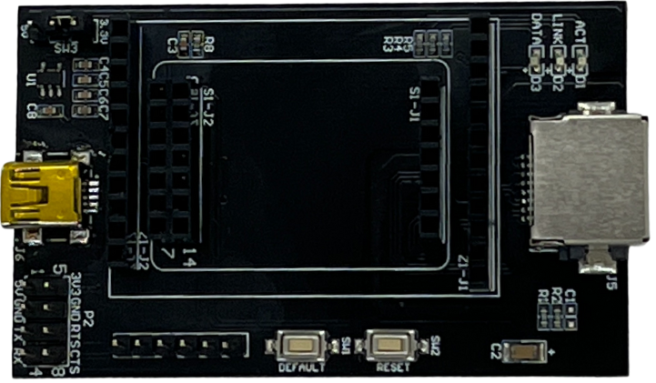
WIZSE Breakout Board
 |
- W5500S2E and W7500S2E Developer board
- RJ45 with external LED status
- Mini USB Power supply
- Power Source selection Pin header
- Serial TTL Pin headers for Serial testing
- Reset and Factory reset button
WIZSE Breakout Board Pinout
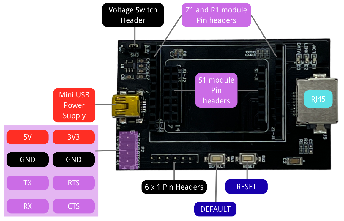 |
WIZSE Breakout Board pin assignments
 |  |
 |  |
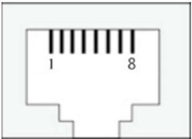
RJ45 (J5) Interface Pin Assignments
"X" indicate for not connected
| Pin | Signal | Pin | Signal |
|---|---|---|---|
| 1 | RXIN | 5 | X |
| 2 | RXIP | 6 | TXOP |
| 3 | TXON | 7 | X |
| 4 | X | 8 | X |
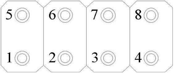
P2 Interface Pin Assignments
"X" indicate for not connected
| Pin | Signal | Pin | Signal |
|---|---|---|---|
| 1 | 5.0V | 5 | 3.3V |
| 2 | GND | 6 | GND |
| 3 | TXD | 7 | RTS |
| 4 | RXD | 8 | CTS |
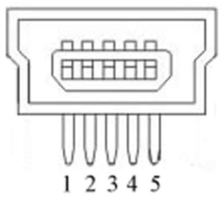
Mini USB (J6) Interface Pin Assignments
"X" indicate for not connected
| Pin | Signal | Pin | Signal |
|---|---|---|---|
| 1 | 5.0V | 4 | X |
| 2 | X | 5 | GND |
| 3 | X | - | - |
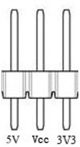
SW3 Power selection Pin Assignments (Jumper selection)
"X" indicate for not connected
| Pin | Signal | Description |
|---|---|---|
| 1 | 5.0V | Short with Vcc for W5500S2E-Z1 |
| 2 | Vcc | Short with 5V or 3V3 for Vcc voltage |
| 3 | 3.3V | Short with Vcc for W5500S2E-S1 |
Schematic
W7500S2E Series
| H/W version | Module | File Type | Link | Remarks |
|---|---|---|---|---|
| 1.2 | W7500S2E-R1 | Lastest H/W version |
Electrical Characteristics
Operating Conditions
The following tables show the voltage and current under 25 °C environment
| Symbol | Parameter | Module | type | Min | Typ | Max | Unit |
|---|---|---|---|---|---|---|---|
| Vin | Module Voltage | W7500S2E-R1 | Voltage Input | 3.0 | 3.3 | 3.6 | V |
| Iin | Module Current | W7500S2E-R1 | Current Input | 61 | 66 | 73 | mA |
| - | Module Current | W7500S2E-R1 | Standby Current | - | 53 | - | mA |
| - | Module Current | W7500S2E-R1 | Normal communication | - | 66 | - | mA |