W55RP20-2S2E
Overview
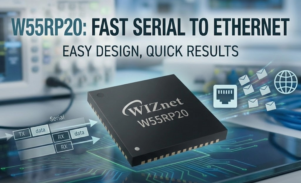
The W55RP20-2S2E is a pre-programmed product with an Serial to Ethernet FW and a valid MAC address into the W55RP20.
WIZnet 2S2E Solution
-
WIZnet 'Serial to Ethernet' product is a protocol converter that transmits data sent by serial equipment as TCP/IP data and converts the TCP/IP data received through the network back into serial data to the serial equipment.
-
With this product, it is possible to easily add an Ethernet networking function to a device supporting UART/SPI interface, the devices can be controlled via an Ethernet network - Internet.
-
The 2S2E version supports dual serial channels, enabling simultaneous communication with two independent serial devices.
-
We also provide Customization Services such as change / add functions by customer request.
Features
The following key features are included with the W55RP20-2S2E product.
- 10/100Mbps Ethernet & Up to 921,600bps serial speed
- Dual Serial to Ethernet channels (2x UART/SPI interfaces)
- Easy to add Ethernet networking function through UART or SPI interface of any device / MCU
- Support RS-232C and RS-422/485 if an external circuit is configured.
- Status pins: PHY link status / TCP connection status / Run status
- Support multiple protocols
- TCP Server
- TCP Client
- SSL TCP Client
- TCP Mixed
- Modbus RTU/ASCII (available only in TCP Server mode)
- UDP (multicast supported)
- MQTT Client
- MQTTS Client
- Support custom protocols (Please submit custom protocol requests via this link.)
- HTTP
- HTTPS
- CoAP
- External device OTA
- Support serial data packing
- Support TCP connection password
- Configuration is possible via serial AT commands or via Configuration tool
- Separate Data UART and Debug UART port
- Unique MAC Address (WIZnet OUI)
Hardware Design Guide & References
Pin Assignment
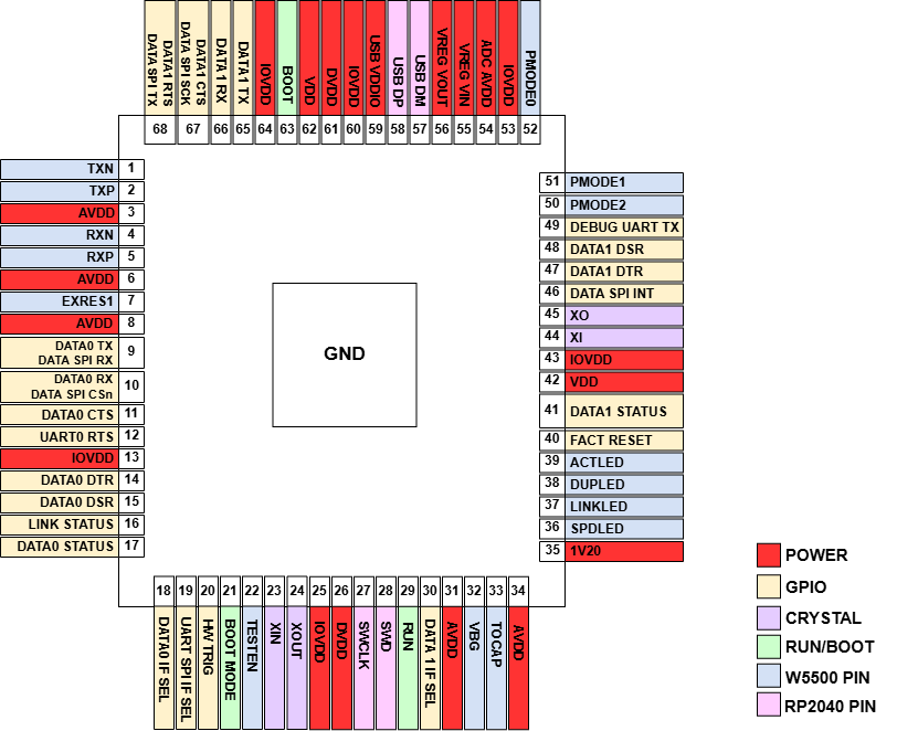
| Pin Number | Signal | Description |
|---|---|---|
| 1 | TXN | TXP/TXN differential signal pair The differential data is transmitted to the media on the TXP/TXN signal pair. |
| 2 | TXP | TXP/TXN differential signal pair |
| 3 | AVDD | TOE Analog 3.3V power |
| 4 | RXN | RXP/RXN differential signal pair The differential data from the media is received on the RXP/RXN signal pair. |
| 5 | RXP | RXP/RXN differential signal pair |
| 6 | AVDD | TOE Analog 3.3V power |
| 7 | EXRES1 | External Resistor pin Connect a resistor of 12.4KΩ to the AGND. (Refer to the “Reference schematic”) |
| 8 | AVDD | TOE Analog 3.3V power |
| 9 | DATA0_TX_PIN / DATA_SPI_RX_PIN | TX pin for Data0 UART transmission (UART Mode) / RX pin for Data SPI reception (SPI Mode) |
| 10 | DATA0_RX_PIN / DATA_SPI_CSn_PIN | RX pin for Data0 UART reception (UART Mode) / SPI Chip Select pin (SPI Mode) |
| 11 | DATA0_CTS_PIN | CTS pin for Data0 UART flow control (UART Mode) |
| 12 | DATA0_RTS_PIN | RTS pin for Data0 UART flow control (UART Mode) |
| 13 | IOVDD | Digital IO Supply Power supply for digital GPIOs, nominal voltage 3.3V |
| 14 | DATA0_DTR_PIN | DTR pin for Data0 UART control |
| 15 | DATA0_DSR_PIN | DSR pin for Data0 UART control |
| 16 | STATUS_PHYLINK_PIN | Output High when the PHY link is established |
| 17 | DATA0_STATUS_TCPCONNECT_PIN | Output High when TCP connection is active |
| 18 | DATA0_IF_SEL | UART0 Interface select pin. High : 485/422, Low or NC : TTL/232 (UART Mode) |
| 19 | UART_SPI_IF_SEL_PIN | UART / SPI Interface select pin. High : SPI, Low or NC : UART |
| 20 | HW_TRIG_PIN | When this pin is Low during a device reset, it enters AT Command Mode |
| 21 | BOOT_MODE_PIN | When this pin is Low during a device reset, it enters Boot Mode |
| 22 | TESTEN | Factory test mode pin Tie to GND. |
| 23 | XIN | Crystal input/output Connect a crystal to RP2040’s crystal oscillator. XIN can also be used as a single-ended CMOS clock input, with XOUT disconnected. The USB bootloader requires a 12MHz crystal or 12MHz clock input. |
| 24 | XOUT | Crystal input/output |
| 25 | IOVDD | Digital IO Supply Power supply for digital GPIOs, nominal voltage 3.3V |
| 26 | DVDD | Digital core power supply Nominal voltage 1.1V. Can be connected to VREG_VOUT, or to some other board-level power supply. |
| 27 | SWCLK | Debug clock/data Access to the internal Serial Wire Debug multi-drop bus. Provides debug access to both processors, and can be used to download code. |
| 28 | SWD | Debug clock/data |
| 29 | RUN | Global asynchronous reset pin Reset when driven low, run when driven high. If no external reset is required, this pin can be tied directly to IOVDD. |
| 30 | DATA1_IF_SEL | DATA1 UART Interface select pin. High : 485/422, Low or NC : TTL/232 (UART Mode) |
| 31 | AVDD | TOE Analog 3.3V power |
| 32 | VBG | Output of band gap |
| 33 | TOCAP | External Reference Capacitor This pin must be connected to a 4.7uF capacitor. The trace length to capacitor should be short to stabilize the internal signals. |
| 34 | AVDD | TOE Analog 3.3V power |
| 35 | 1V2O | 1.2V regulator output voltage Connect 10nF capacitor. |
| 36 | SPDLED | Speed LED This shows the Speed status of the connected link. Low: 100Mbps High: 10Mbps |
| 37 | LINKLED | Link LED This shows the Link status. Low: Link is established High: Link is not established |
| 38 | DUPLED | Duplex LED This shows the Duplex status for the connected link. Low: Full-duplex mode High: Half-duplex mode |
| 39 | ACTLED | Active LED This shows that there is Carrier sense (CRS) from the active Physical Medium Sub-layer (PMD) during TX or RX activity. Low: Carrier sense from the active PMD High: No carrier sense |
| 40 | FAC_RSTn_PIN | Holding Low for more than 5 seconds triggers a factory reset |
| 41 | DATA1_STATUS_TCPCONNECT_PIN | Output High when TCP connection is active |
| 42 | VDD | TOE Digital 3.3V Power |
| 43 | IOVDD | Digital IO Supply Power supply for digital GPIOs, nominal voltage 3.3V |
| 44 | XI | 25MHz crystal input/output A 25MHz crystal and oscillator is used to connect these pins. |
| 45 | XO | 25MHz crystal input/output A 25MHz crystal and oscillator is used to connect these pins. |
| 46 | DATA_SPI_INT_PIN | SPI Master Recv data pending pin |
| 47 | DATA1_DTR_PIN | DTR pin for Data1 UART control |
| 48 | DATA1_DSR_PIN | DSR pin for Data1 UART control |
| 49 | Debug_UART_TX_PIN | Output Debug Messages |
| 50 | PMODE2 | PHY Operation mode select pins. Default: Pull-up (77kΩ) |
| 51 | PMODE1 | PHY Operation mode select pins. Default: Pull-up (77kΩ) |
| 52 | PMODE0 | PHY Operation mode select pins. Default: Pull-up (77kΩ) |
| 53 | IOVDD | Digital IO Supply Power supply for digital GPIOs, nominal voltage 3.3V. |
| 54 | ADC_AVDD | ADC supply Power supply for analogue-to-digital converter, nominal voltage 3.3V. |
| 55 | VREG_VIN | Voltage regulator input supply Power input for the internal core voltage regulator, nominal voltage 1.8V to 3.3V. |
| 56 | VREG_VOUT | Voltage regulator output Power output for the internal core voltage regulator, nominal voltage 1.1V, 100mA max current. |
| 57 | USB_DM | USB controller, supporting Full Speed device and Full/Low Speed host. A 27Ω series termination resistor is required on each pin, but bus pull-ups and pull-downs are provided internally. |
| 58 | USB_DP | USB controller |
| 59 | USB_VDD | USB supply Power supply for internal USB Full Speed PHY, nominal voltage 3.3V |
| 60 | IOVDD | Digital IO Supply Power supply for digital GPIOs, nominal voltage 3.3V |
| 61 | DVDD | Digital core power supply, nominal voltage 1.1V. Can be connected to VREG_VOUT, or to some other board-level power supply |
| 62 | VDD | Power supply of the Flash Memory |
| 63 | BOOT | BOOT Pin When power is applied and during reset, if the BOOT pin is low, the device enters BOOTSEL mode. |
| 64 | IOVDD | Digital IO Supply Power supply for digital GPIOs, nominal voltage 3.3V |
| 65 | DATA1_TX_PIN | Output Debug Messages |
| 66 | DATA1_RX_PIN | Input Debug Messages |
| 67 | DATA1_CTS_PIN / DATA_SPI_SCK_PIN | SCK Input pin for Data SPI transmission (SPI Mode) |
| 68 | DATA1_RTS_PIN / DATA_SPI_TX_PIN | TX pin for Data SPI transmission (SPI Mode) |
**BOOT_MODE pin is for Entering W55RP20-2S2E BOOT mode and BOOT pin is for Entering RP2040 core BOOT mode.
Manuals
- How to use Config-tool
- How to use Web config
- How to use AT CMD
- How to connect MQTT
- How to connet SSL
- How to connet Modbus
- How to upload/update FW
- How to do factory reset
- How to write MAC Address
- How to design hardware
- How to use SPI Mode
Customization Services
WIZnet offers Customization services for your specific needs.
We can provide customization services based on W55RP20-2S2E chip products: Depending on the customer application, it is possible to change the initial settings of the product, change the MAC address, add various protocols, and add functions. The developed firmware is programmed into the W55RP20 MCU and delivered to the requesting customer.
We also provide technical support including various hardware guide and references for customer's quick product design-win.