EOE-ioNIC Datasheet [EN]
Overview
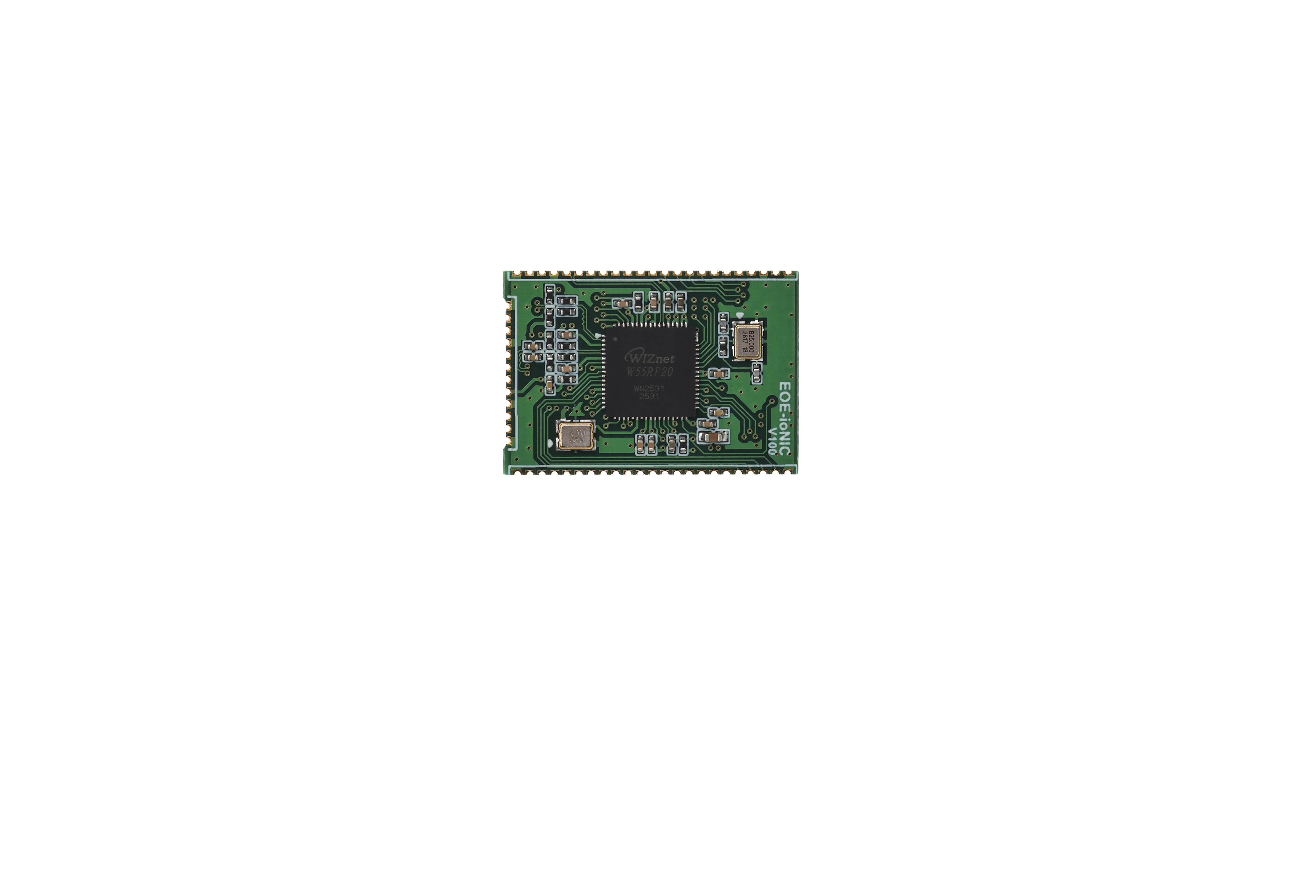
This document is the hardware specification for the EOE-ioNIC, a serial-to-Ethernet System-on-Module (SoM) based on the W55RP20 — WIZnet's single-package solution combining the Raspberry Pi RP2040 dual-core MCU with the W5500 hardwired TCP/IP (Ethernet Offload Engine) controller and 2 MB of flash.
The EOE-ioNIC is a solder-down module intended to be mounted on a customer carrier board. It brings the Ethernet MDI pair, both UART channels, the SPI host interface, USB and SWD out to a 70-pin castellated edge interface. For an out-of-the-box evaluation platform that adds an RJ45 jack, USB Type-C, DC jack and headers, see the EOE-ioNIC-EVB.
The EOE-ioNIC is a module, not a finished board. It has no RJ45 jack, no USB connector, no DC jack, no push buttons and no on-board 3.3V regulator — those belong to the carrier board. The module is powered directly from a 3.3V rail.
Features
- W55RP20-based module (RP2040 dual-core Arm Cortex-M0+ MCU + W5500 hardwired TCP/IP core + 2 MB flash)
- Hardwired TCP/IP protocols: TCP, UDP, ICMP, IPv4, ARP, IGMP, PPPoE
- 10/100 Mbps Ethernet with the complete on-module MDI front-end (termination, series matching and bandgap reference resistors); requires only external RJ45 magnetics
- Dual UART channels with full modem control (RX / TX / RTS / CTS / DSR / DTR)
- UART or SPI host interface, selected by the
SPI_IF_SELpin - Per-channel status outputs:
STATUS0_PHY,STATUS0_TCP,STATUS1_TCP - Ethernet PHY status outputs:
LINK,ACT,SPD,DUP— each also drives an on-module green indicator LED through a 330 Ω series resistor - On-module clocks: 12 MHz oscillator for the RP2040 core and a 25 MHz crystal for the Ethernet PHY — no external clock required
- Single 3.3V supply; the 1.1V core rail is generated by the W55RP20 internal regulator
- Control pins brought out to the edge interface:
RSTn,RP_BOOT(RP2040 BOOTSEL),FW_BOOT(S2E firmware boot),FACT_RSTn(factory reset),HW_TRIG(AT command mode),DEBUG - Interface-select pins:
SPI_IF_SEL,UART0_IF_SEL,UART1_IF_SEL - Native USB (
D_P/D_N) for firmware upload in BOOTSEL mode - SWD debug port (
SWCLK/SWD) - 70-pin castellated edge interface on all four sides
Electrical Specification
| Item | Symbol | Min | Typ | Max | Unit | Remarks |
|---|---|---|---|---|---|---|
| Supply voltage | VDD | 3.0 | 3.3 | 3.6 | V | Single rail; core 1.1V generated internally |
| I/O level | — | — | 3.3 | — | V | TTL, not 5V tolerant |
| Operating temperature | TA | −40 | — | +85 | ℃ | |
| Storage temperature | TS | −40 | — | +85 | ℃ | |
| Supply current | IDD | — | TBD | TBD | mA |
All module I/O is 3.3V TTL and is not 5V tolerant. Level-shift any 5V host signals on the carrier board.
Power Supply
The module takes a single 3.3V input on pins 48 / 49 / 50. The W55RP20's internal regulator derives the 1.1V core rail, which is decoupled on-module — no external core supply or additional regulator is required on the carrier board.
Decoupling for the 3.3V rail is provided on-module. On the carrier board, place bulk capacitance close to the module's 3.3V pins and keep the return path to the GND pins short.
Reset
RSTn is active low and is pulled up to 3.3V on-module through a 4.7 kΩ resistor with an
RC delay capacitor. It is available on both pin 51 (right side) and pin 62 (top side); the
two are the same net. If the carrier board does not drive reset, both pins may be left open.
Hardware Specification
Clocks
| Reference | Frequency | Function |
|---|---|---|
| Y1 | 12 MHz | RP2040 core clock (oscillator, drives XIN) |
| Y2 | 25 MHz | W5500 Ethernet PHY clock (crystal with 18 pF load capacitors) |
Both clock sources are fitted on the module. No external clock input is needed.
Ethernet MDI Interface
The module implements the full W5500 analog front end: 49.9 Ω 1% differential termination, 3.3 Ω series matching resistors on each MDI line, and the 12.4 kΩ 1% bandgap reference. The carrier board only has to provide the RJ45 magnetics (or a magnetics-integrated RJ45 jack) and the cable-side termination.
| Module pin | Signal | Connect to |
|---|---|---|
| 25 | MDI_T_P | Transformer transmit pair + |
| 26 | MDI_T_N | Transformer transmit pair − |
| 28 | TCT | Transmit center tap |
| 31 | RCT | Receive center tap |
| 33 | MDI_R1_P | Transformer receive pair + |
| 34 | MDI_R1_N | Transformer receive pair − |
Typical RJ45 wiring on the carrier board (cable side of the magnetics):
| RJ45 pin | Signal | Description |
|---|---|---|
| 1 | TXP | TX+ |
| 2 | TXN | TX− |
| 3 | RXP | RX+ |
| 4 | — | Unused (or PoE pair) |
| 5 | — | Unused (or PoE pair) |
| 6 | RXN | RX− |
| 7 | — | Unused (or PoE pair) |
| 8 | — | Unused (or PoE pair) |
The EOE-ioNIC does not include PoE. If PoE is required it must be implemented on the carrier board; when it is, pins 4/5 and 7/8 must carry opposite polarity.
Status LED Signals
LINK, ACT, SPD and DUP are driven directly by the W5500 PHY and each already
drives a green LED on the module through a 330 Ω resistor. The same signals are also
routed to the edge interface so the carrier board can repeat them.
| Module pin | Signal | Indication |
|---|---|---|
| 47 | LINK | Ethernet link established |
| 46 | ACT | Transmit / receive activity |
| 38 | SPD | 100 Mbps (asserted) / 10 Mbps |
| 37 | DUP | Full duplex (asserted) / half duplex |
When repeating these signals with an additional LED on the carrier board, size the series resistor for the extra load — the module LED is already drawing from the same PHY pin.
Control and Mode-Select Pins
These are pins, not switches or buttons. Drive them from the carrier board (jumper, push button, or host GPIO) as required.
| Module pin | Signal | Function |
|---|---|---|
| 51 / 62 | RSTn | Active-low reset (4.7 kΩ pull-up on-module) |
| 41 | RP_BOOT | RP2040 BOOTSEL — hold low at reset to enumerate as a USB mass-storage device |
| 13 | FW_BOOT | Enter W55RP20-S2E firmware boot mode (active low) |
| 40 | FACT_RSTn | Factory reset — drive low for ≥ 5 s to restore factory settings |
| 12 | HW_TRIG | Low: AT command mode / High: gateway mode |
| 17 | DEBUG | Debug UART enable |
| 11 | SPI_IF_SEL | High: SPI host interface / Low or NC: UART host interface |
| 10 | UART0_IF_SEL | UART0 interface select (TTL/232 vs 485/422) |
| 14 | UART1_IF_SEL | UART1 interface select (TTL/232 vs 485/422) |
USB Interface
D_P (pin 19) and D_N (pin 18) are the W55RP20's native USB lines — there is no
USB-to-UART bridge on the module. Route them as a 90 Ω differential pair on the carrier
board and fit the usual series termination and a USB connector.
The USB interface is used to upload and update the firmware after the W55RP20 enters
BOOTSEL mode (RP_BOOT low at reset). For detailed instructions, see the FW update guide
in the Manuals section.
SWD / Debug Interface
| Module pin | Signal | Description |
|---|---|---|
| 67 | SWCLK | Serial Wire Debug clock |
| 68 | SWD | Serial Wire Debug data |
| 62 | RSTn | Reset (shared with pin 51) |
Pin-out
The complete 70-pin edge-interface diagram will be added when the pinout image is available.
Dimension
| TBD |
| EOE-ioNIC Revision 1.0 Dimension |
- TBD (mm)
Manuals
| Title | Description | Link | Notes |
|---|---|---|---|
| Configuration Tool Manual | How to use the configuration tool | EN | - |
| Command Manual | AT command reference | - | TBD |
| FW Update Guide | Firmware update over USB BOOTSEL | - | TBD |
Certification
- TBD
Design file
Schematic
| H/W version | Filetype | Download Link | Remarks |
|---|---|---|---|
| 1.0 | Altium | TBD | - |
| ::: | TBD | ::: |
Part list
| H/W version | Filetype | Download Link | Remarks |
|---|---|---|---|
| 1.0 | Excel | TBD | - |
| ::: | TBD | ::: |
3D file
| H/W version | Filetype | Download Link | Remarks |
|---|---|---|---|
| 1.0 | STEP | TBD | - |