Hardware Design Guide
Summary
This document is a Design Guide for WIZnet Chip to be used for PCB. It contains reference for PCB design using W5100, W5300, W5500, W7100A, W7500, and W7500P. Contents of MDI (Medium-dependent interface) signal, power supply, parts placement, MII (Media Independent Interface), etc. are included and you must follow the instructions below. If you do not follow the instructions, you are likely to experience degraded Ethernet performance.
MDI signal Schematic
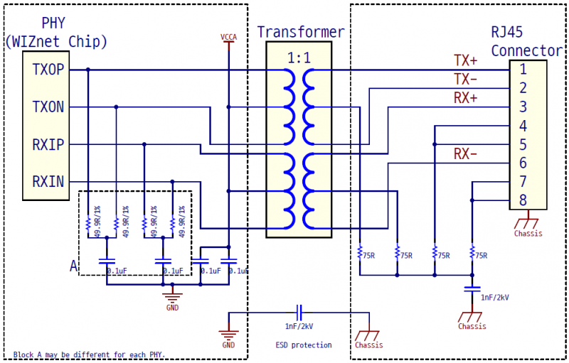
- The above circuit is the most used for Ethernet implementation.
- W5100, W5300, W7100 should be configured as shown above.
- For the W5500, please follow the URL below for your reference.
- Since the W7500 must use an external PHY, you should contact the manufacturer of PHY you are using.
- W7500P has built in PHY, and the circuit should be constructed by removing part A from the above diagram.
Parts Placement
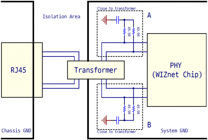
- Place A and B parts as close as possible to the Transformer.
- If you are using a RJ-45 Connector which is separated from the
Transformer, you should place both as close to each other as
possible.
- Distance must be more than 2.5mm (100mil) and less than 25mm (1000mil).
- All PCB layers under the Transformer and RJ45 Connector must have no power and GND plane.
- Between PHY and RJ45 Connector, there should be no routing for a
digital signal.
- Prevention of signal interference.
- There should be no high-frequency device and routing near the TX+/-
and RX+/- signals.
- Prevention of signal interference.
- We generally recommend you to use a connector that combines a Transformer and RJ-45 Connector.
- High electric currents cause to increase EMI noise; therefore do not place the devices near that consume high currents.
- Place the Crystal and Oscillator as close as possible.
Power supply & GND
- Connect the RJ-45 connector Shield to Chassis GND.
- External ESD protection.
- Separate Chassis GND and System GND by 1nF/200V Capacitor.
- External ESD protection.
- Make GND as wide as possible.
- The analog GND pin and digital GND pin should be maintained in a
good path.
- We recommend you not to separate analog and digital GND.
- In some cases, such as the W5100 and W5300 reference circuits, DGND and AGND can be separated by beads, but if there is enough GND space, it is better to integrate them into DGND than to separate them by beads.
- Place a 0.1uF Bypass Capacitor near the input pin to reduce noise
from power supply.
- Place as close as possible to the input pin through the Bypass Capacitor.
- Place additional 10uF, 4.7uF Capacitors.
- Input power through Ferrite Bead or 0 Ohm Resistor.
- Functions as power filter and blocks noise.
- Use a 3.3V Regulator with at least 300mA output current.
- We recommend you to design one power Plane and GND for PCB to input low Impedance power.
MDI routing
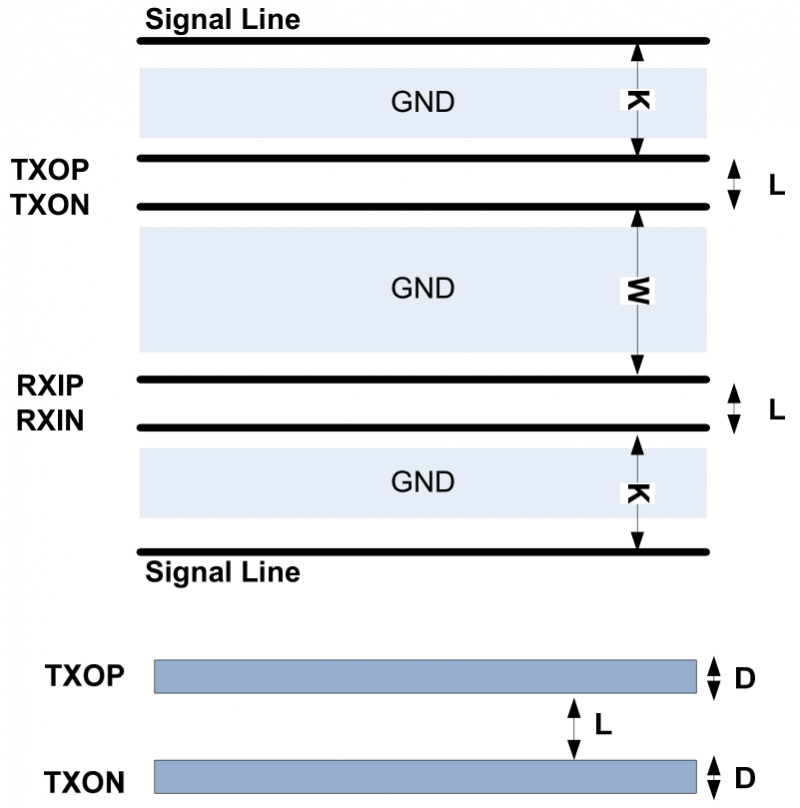
| Min | Typ | MAX | Descriptions | |
|---|---|---|---|---|
| D | 6mil | - | 12mil | TX+/- and RX+/- Trace thickness, ex) 8mil |
| L | - | - | 10mil | Distance between +/- Differential signal, ex) 4mil |
| W | 20mil | - | - | Distance between TX+/- and RX+/- signals, ex) 30mil |
| K | 20mil | - | - | Distance between TX+/- and RX+/- signals and others & power, ex) 30mil, separate by GND. |
- The MDI (medium-dependent interface) signal is connected to the RJ-45 Connector through the Transformer.
- The individual impedance of the TX+/- and RX+/- signals is kept
below 50Ω.
- Impedance of +/- Differential signal should be maintained at 100Ω.
- Connect TX+/- and RX+/- signals as short as possible.
- Recommended signal length is less than 25mm (1000 mil).
- In worst case, MDI maximum routing length is 75mm (3000mil).
- Connect TX+/TX- and RX+/RX- with the same length as possible.
- +/- Differential signal should be same length.
- Timing problems may occur depending on the Trace length.
- Wire connections between TX+/- and RX+/- are prohibited.
- If necessary, use a twisted cable to connect as short as possible. (75mm or less)
- Routing for TX+/- and RX+/- should be connected at 45° or curved lines except 90°.
- TX+/- and RX+/- signals prohibit Via or Layer changes.
MII routing (Only W7500)
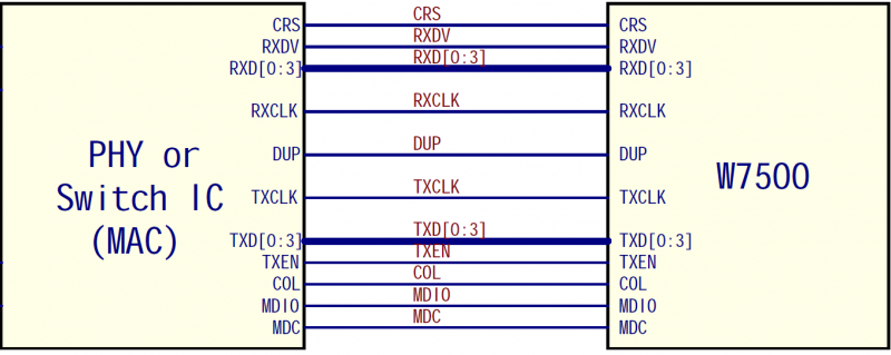
- MII (Media Independent Interface) connects to the PHY MAC (Media Access Controller).
- MII is a bus signal that needs to be maintained 68 Impedance according to the IEEE specification.
- MII Data signals (RXD[0:3], TXD[0:3]) should be routed as close as possible.
- MII Clock signals (RX_CLK, TX_CLK) should be routed at enough distance from the data signal.
- Trace length should be as short as possible.
- Trace length should be less than 150mm(6000mil).
- If the Trace length is long, it becomes vulnerable to external noise, and it causes EMI emission, also it is highly to interfere with external signals.
- All Trace length difference should be less than 50mm(2000mil).
- Timing problems may occur depending on the length of Trace.
- Routing for Data and Clock signals should be connected at 45° or curved lines except 90°.
- Data and Clock signals prohibit Via or Layer changes
- Must be routed in the same GND Plane.
ESD & EMI
- Chassis GND and System GND should be separated more than 80mil.
- Protect the circuit from external ESD shocks by using TVS diode.
- Use a metal RJ45 Connector.
- Connect Shield to Chassis GND.
ETC
- In case of using 25MHz crystal, use a 50ppm crystal or less.