Datasheet
Hardware Specification
Product Spec Table
| Category | Description | Description |
|---|---|---|
| MCU | Arm® 32-bit Cortex®-M33 CPU with TrustZone® and FPU | 48Mhz maximum frequency Internal 16Mhz RC Oscillator Flash: 512KB 256 Kbytes of SRAM including 64 Kbytes with hardware parity check Arm® TrustZone® and securable I/Os, memories and peripherals 512-byte OTP (one-time programmable) for user data |
| MCU | Hardwired TCP/IP Core | 4 independent Sockets SRAM for socket: 32KB MII (Medium-Independent Interface) TCP/IP Protocols: TCP, UDP, ICMP, IPv4, ARP, IGMP, PPPoE |
| MCU | PHY | IC+(IP101G) PHY Auto negotiation (Full-duplex and Half-duplex) Auto MDI/MDIX |
| Serial | Interface | WIZ510SSL |
| Serial | Signal | TXD, RXD, RTS, CTS, GND |
| Serial | Parameters | Parity: None, Odd, Even Data bits: 7, 8 bit Flow control: None, RTS / CTS, XON / XOFF |
| Serial | Speed | Up to 460Kbps |
| Dimension | ( PCB board size ) ( Include part size ) | |
| Connector type | TBC 2.54mm Pitch 1x12 Pin-header(Data Line) 2.54mm Pitch 1x12 Pin-header(ISP) 2.54mm Pitch 1x12 Pin-header(Expansion GPIO & app_boot) 1.27mm Pitch 1x5 Pin-header (JTAG) | |
| Input Voltage | DC 3.3V | |
| Temperature | TBC 0℃ ~ 70℃ (Operation), -40℃ ~ 85℃ (Storage range) |
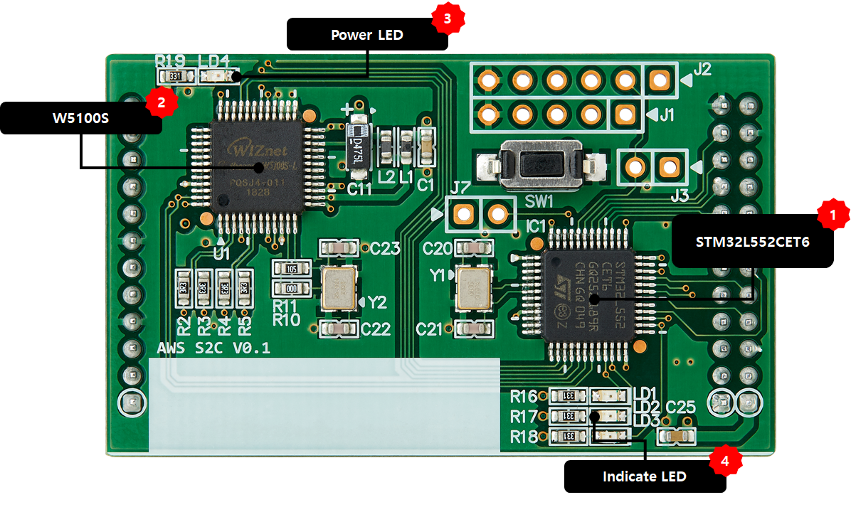
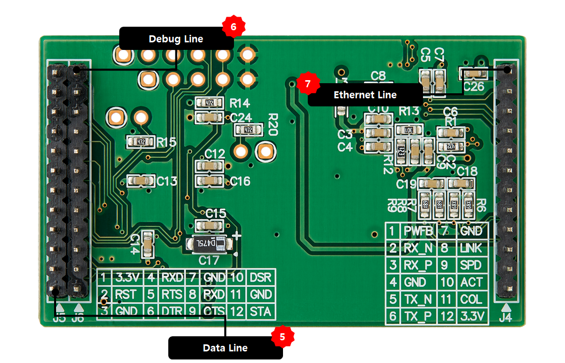
Callout
Rev1.0
 |  |
| TOP | BOTTOM |
Schematic
| H/W version | Type | Filetype | Download Link | Remarks |
|---|---|---|---|---|
| 1.0 | RS-232 | Altium | Coming soon | - |
| ::: | ::: | - |
Part list
| H/W version | Filetype | Download Link | Remarks |
|---|---|---|---|
| 1.0 | Excel | Download | |
| Download |
Electrical Characteristics
Operating Conditions
| Symbol | Parameter | Pins | Min | Typ | Max | Unit |
|---|---|---|---|---|---|---|
| Vcc | Operating Voltage | 3.3V | 3.135 | 3.3 | 3.6 | V |
| Vss | Ground | ALL | 0 | 50 | mV | |
| fFCLK | Internal CPU clock frequency | ALL | 0 | - | 48 | MHz |
| Tstg | Storage Temperature (max) | ALL | -40 | 85 | ℃ | |
| TA | Ambient operating temperature | ALL | -40 | 85 | ℃ | |
| VIO | I/O Signal voltage (Tolerance) | ALL | Vss-0.3 | 3.3 | 5 | V |
| VIH | Input high voltage | ALL | 2.5 | V | ||
| VIL | Input low voltage | ALL | 0.6 | V | ||
| VOH | Output high voltage (High driving strength Current load = 6mA) (Low driving strength Current load = 3mA) | ALL | 2.83 | V | ||
| VOL | Output high voltage (High driving strength Current load = 6mA) (Low driving strength Current load = 3mA) | ALL | 0.32 | V |
Absolute maximum ratings
Voltage characteristics
| Symbol | Ratings | Min | Max | Unit |
|---|---|---|---|---|
| VDDX-VSS | External main supply voltage (including VDD, VDDA, VDDIO2, VDDUSB, VBAT, VDDSMPS, VREF+) | -0.3 | 4.0 | V |
| VDD12-VSS | External SMPS supply voltage (All ranges 0/1/2) | -0.3 | 1.4 | V |
| VIN | Input voltage on FT_xxx pins except FT_c pins | VSS-0.3 | min (VDD, VDDA, VDDIO2, VDDUSB, VDDSMPS) + 4.0 | V |
| :: | Input voltage on FT_c pins | VSS-0.3 | 5.5 | V |
| :: | Input voltage on any other pins | VSS-0.3 | 4.0 | V |
| VREF+-VDDA | Allowed voltage difference for VREF+ > VDDA | - | 0.4 | V |
| |∆VDDX| | Variations between different VDDX power pins of the same domain | - | 50 | mV |
| |VSSX-VSS| | Variations between all the different ground pins | - | 50 | mV |
Current characteristics
| Symbol | Ratings | Max | Unit |
|---|---|---|---|
| ∑IVDD T | Total current into sum of all VDD power lines (source) | 160 | mA |
| ∑IVSS | Total current out of sum of all VSS ground lines (sink) | 160 | mA |
| IVDD(PIN) | Maximum current into each VDD power pin (source) | 100 | mA |
| IVSS(PIN) | Maximum current out of each VSS ground pin (sink) | 100 | mA |
| IIO(PIN) | Output current sunk by any I/O and control pin except FT_f | 20 | mA |
| :: | Output current sunk by any FT_f pin | 20 | mA |
| :: | Output current sourced by any I/O and control pin | 20 | mA |
| ∑IIO(PIN) | Total output current sunk by sum of all I/Os and control pins | 100 | mA |
| :: | Total output current sourced by sum of all I/Os and control pins | 100 | mA |
| IINJ(PIN) | Injected current on FT_xxx, TT_xx, RST and B pins, except PA4, PA5 | -5/+0 | mA |
| :: | Injected current on PA4, PA5 | -5/0 | mA |
| ∑|IINJ(PIN)| | Total injected current (sum of all I/Os and control pins) | +/-25 | mA |
Thermal characteristics
| Symbol | Ratings | Max | Unit |
|---|---|---|---|
| TSTG | Storage temperature range | -65 to +150 | ℃ |
| TJ | Maximum junction temperature | 150 | ℃ |
Flash Memory
| Symbol | Parameter | Conditions | Min(1) | Unit |
|---|---|---|---|---|
| NEND | Sector Endurance | TA = –40 to +105 °C | 10,000 | Cycles |
| TDR | Data Retention | 1 kcycle(2) at TA = 85 °C 1 kcycle(2) at TA = 105 °C 1 kcycle(2) at TA = 125 °C 1 kcycle(2) at TA = 55 °C 1 kcycle(2) at TA = 85 °C 1 kcycle(2) at TA = 105 °C | 30 15 7 30 15 10 | Years |
(1) - Guaranteed by characterization results. (2) - Cycling performed over the whole temperature range.
Ethernet Power Dissipation
WIZ510SSL-TTL
| Condition | Min | Typ | Max | Tol | Unit |
|---|---|---|---|---|---|
| 100M Link | - | 67 | - | ±3 | mA |
| 10M Link | - | 52 | - | mA | |
| Unlink (Auto-negotiation mode) | 45 | 50 | 57 | ±3 | mA |
| 100M Transmitting | - | 74 | - | ±3 | mA |
| 10M Transmitting | - | 62 | - | mA |
WIZ510SSL Pinout
1x6 Pin Header
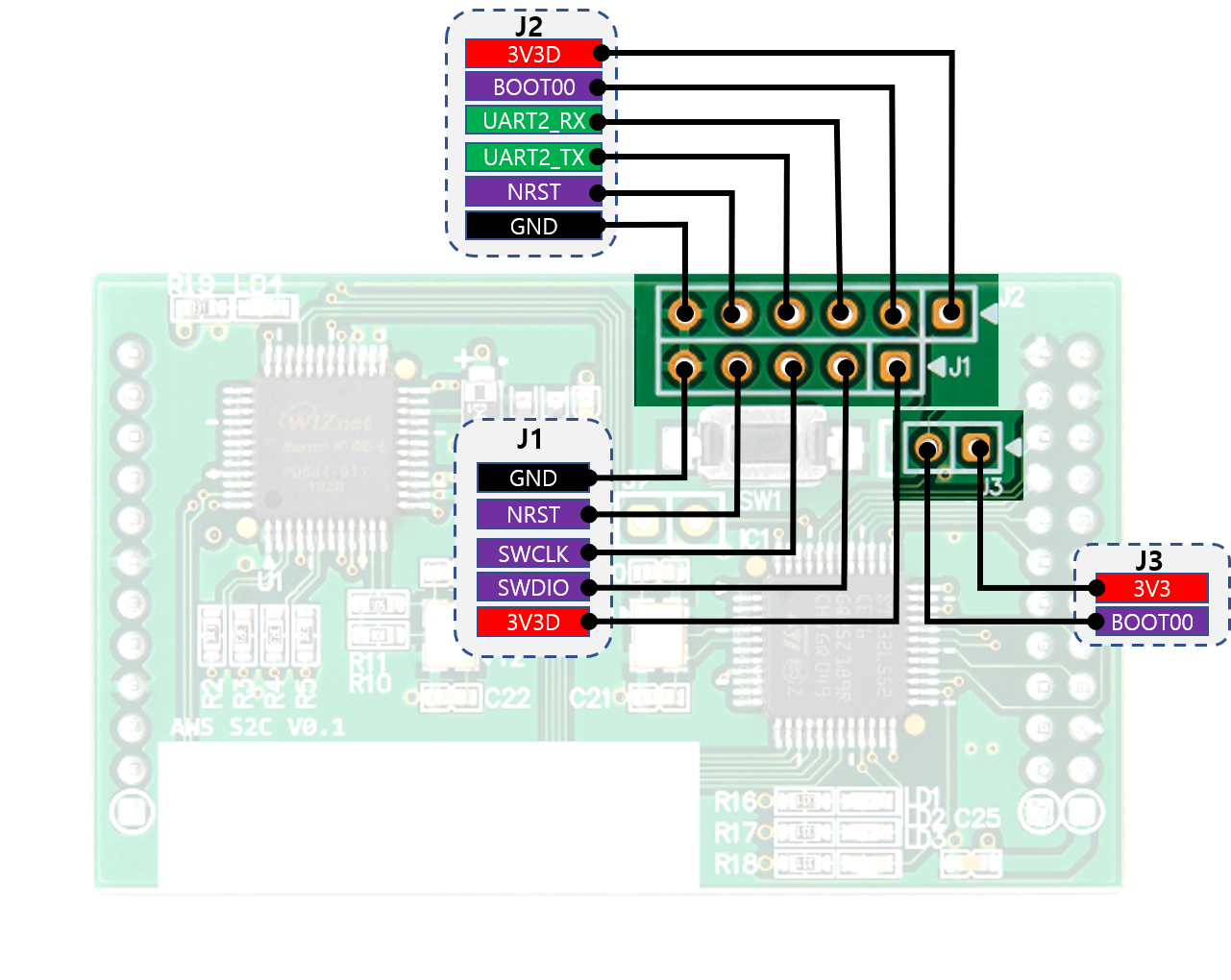
J1 Pin
| Pin Number | Signal |
|---|---|
| 1 | 3V3D |
| 2 | SWDIO |
| 3 | SWCLK |
| 4 | NRST |
| 5 | GND |
J2 Pin
| Pin Number | Signal |
|---|---|
| 1 | 3V3D |
| 2 | BOOT0 |
| 3 | UART2_TX |
| 4 | UART2_RX |
| 5 | NRST |
| 6 | GND |
J3 Pin
| Pin Number | Signal |
|---|---|
| 1 | 3V3D |
| 2 | BOOT0 |
1x12 Pin Header
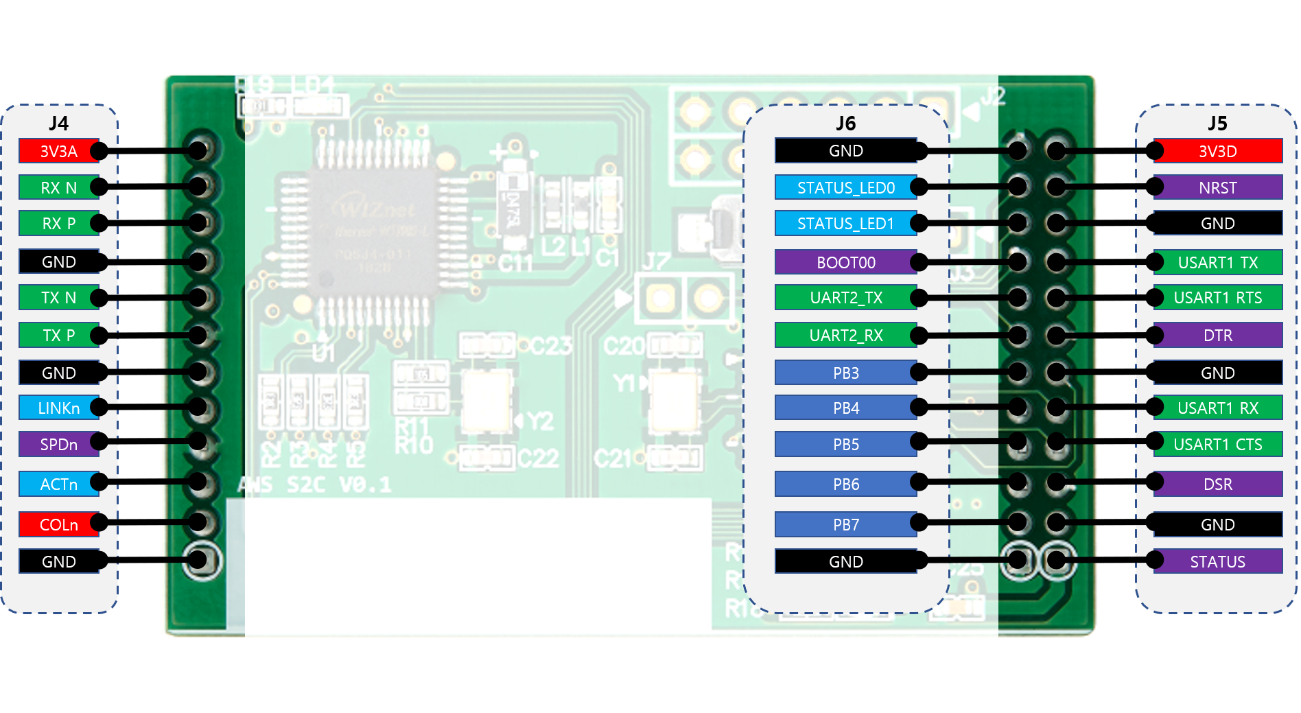
J4 Ethernet Line
| Pin Number | Signal |
|---|---|
| 1 | 3V3A |
| 2 | RX N |
| 3 | RX P |
| 4 | GND |
| 5 | TX N |
| 6 | TX P |
| 7 | GND |
| 8 | LINKn |
| 9 | SPDn |
| 10 | ACTn |
| 11 | COLn |
| 12 | 3V3D |
J5 Data Line
| Pin Number | Signal |
|---|---|
| 1 | 3V3D |
| 2 | NRST |
| 3 | GND |
| 4 | USART1_TX |
| 5 | USART1_RTS |
| 6 | DTR |
| 7 | GND |
| 8 | USART1_RX |
| 9 | USART1_CTS |
| 10 | DSR |
| 11 | GND |
| 12 | STATUS |
J6 Debug Line
| Pin Number | Signal |
|---|---|
| 1 | GND |
| 2 | STATUS LED0 |
| 3 | STATUS LED1 |
| 4 | BOOT00 |
| 5 | UART2 TX |
| 6 | UART2 RX |
| 7 | PB3 |
| 8 | PB4 |
| 9 | PB5 |
| 10 | PB6 |
| 11 | PB7 |
| 12 | GND |
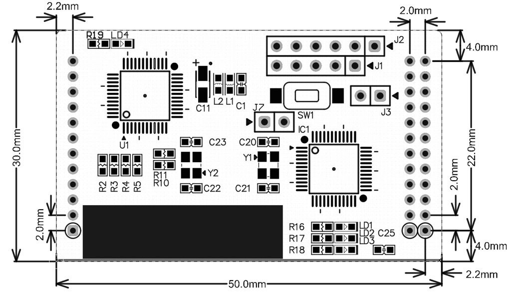
WIZ510SSL Dimension
- WIZ510SSL Dimension :
- 50mm x 30mm ( PCB board size )
 |
| Rev0.1 |