Electrical Characteristics
For details, please refer to W55MH32 Datasheet
Absolute maximum ratings
Loads placed on a device that exceed the values given in the 'Absolute Maximum Ratings' list may result in permanent damage to the device. These are stress ratings only and functional operation of the device at these conditions is not implied. Exposure to maximum rating conditions for extended periods may affect device reliability.
Voltage characteristics
| Symbol | Description | Min | Max | Unit |
|---|---|---|---|---|
| VDD – VSS | External main supply voltage(including VDDA and VDD)(1) | -0.3 | 3.63 | V |
| VIN | Input voltage on 5V tolerant pin(2) | Vss-0.3 | Vdd+4.0 | |
| Input voltage on any other pin(2) | Vss-0.3 | 4.0 | ||
| |ΔVDDx| | Variations between different VDD power pins | — | 50 | mV |
| |VSSx-VSS| | Variations between all the different ground pins | — | 50 |
(1) All main power (VDD, VDDA) and ground (VSS, VSSA) pins must always be connected to the external power supply, in the permitted range.
(2) Contains the VREF-feet.
Current characteristics
| Symbol | Description | Max (1) | Unit |
|---|---|---|---|
| IVDD | Total current into VDD/VDDA power lines (source) (1) | 150 | mA |
| IVSS | Total current out of VSS ground lines (sink) (1) | 150 | |
| IIO | Output current sunk by any I/O and control pin | 25 | |
| Output current source by any I/Os and control pin | -25 |
(1) All main power (VDD, VDDA) and ground (VSS, VSSA) pins must always be connected to the external power supply, in the permitted range.
Thermal Characteristics
| Symbol | Description | Value | Unit |
|---|---|---|---|
| TSTG | Storage temperature range | -65 ~ +150 | ℃ |
| TJ | Maximum junction temperature | 105 | ℃ |
Operating conditions
General operating conditions
| Symbol | Parameter | Condition | Min | Max | Unit |
|---|---|---|---|---|---|
| fHCLK | Internal AHB clock frequency | — | 0 | 216 | MHz |
| fPCLK1 | Internal APB1 clock frequency | — | 0 | 108 | |
| fPCLK2 | Internal APB2 clock frequency | — | 0 | 216 | |
| VDD | Standard operating voltage | — | 2.0 | 3.6 | V |
| VDDA(1) | Analog part operating voltage | Must be same with VDD (1) | 2.0 | 3.6 | V |
| VBAT | Backup part operating voltage | 1.6 | 3.6 | V | |
| TA | Ambient temperature | — | -40 | 85 | ℃ |
(1) It is recommended to power VDD and VDDA from the same source.
Supply current characteristics
The current consumption is a composite indicator of several parameters and factors such as the operating voltage, ambient temperature, I/O pin loading, device software configuration, operating frequencies, I/O pin switching rate, program location in memory and executed binary code, etc.
The current consumption is measured as described in the Test Conditions chapter.
Current consumption
The MCU is placed under the following conditions:
l All I/O pins are in analog input mode.
l All peripherals are disabled except when explicitly mentioned
l When the peripherals are enabled: fPCLK1 = fHCLK/2,fPCLK2 = fHCLK
Table 15 Current consumption in Run mode
| Symbol | Parameter | Conditions | fHCLK | Typ(1) | Max(2) | Unit | ||
|---|---|---|---|---|---|---|---|---|
| All peripherals enabled | All peripherals disabled | All peripherals enabled | All peripherals disabled | |||||
| IDD | Supply current in Run mode | External clock(3) | 216MHz | 36.29 | 25.49 | 38.50 | 27.56 | mA |
| 168MHz | 27.71 | 19.27 | 29.95 | 21.35 | ||||
| 72MHz | 13.09 | 9.38 | 14.93 | 11.21 | ||||
| 48MHz | 9.35 | 6.93 | 11.18 | 8.74 | ||||
| 32MHz | 6.88 | 5.25 | 8.68 | 7.04 | ||||
| 24MHz | 5.67 | 4.46 | 7.41 | 6.20 | ||||
| 16MHz | 4.43 | 3.63 | 6.16 | 5.34 | ||||
| 8MHz | 3.28 | 2.58 | 4.98 | 4.54 | ||||
| Runs on high-speed internal RC oscillator (HSI) | 128MHz | 21.64 | 15.19 | 23.89 | 17.27 | mA | ||
| 72MHz | 13.03 | 9.39 | 15.03 | 11.31 | ||||
| 48MHz | 9.34 | 6.92 | 11.26 | 8.78 | ||||
| 32MHz | 7.55 | 5.73 | 8.73 | 7.08 | ||||
| 24MHz | 5.69 | 4.49 | 7.74 | 6.24 | ||||
| 16MHz | 4.45 | 3.66 | 6.21 | 5.39 | ||||
| 8MHz | 3.30 | 3.88 | 5.02 | 4.57 |
(1) The typical value is obtained by testing at TA=25℃, VDD=3.3V.
(2) The maximum value is obtained by testing at TA=85℃, VDD=3.6V.
(3) The external clock is 8MHz, and the PLL is enabled when fHCLK>8MHz.
General input/output characteristics
I/O static characteristics
| Symbol | Parameter | Conditions | Min | Typ | Max | Unit |
|---|---|---|---|---|---|---|
| VIL | Low level input voltage | — | — | 1.38 | V | |
| VIH | Standard IO input high level voltage | 1.59 | — | — | ||
| IO FT input high level voltage | 1.59 | — | — | |||
| Vhys | Standard IO Schmitt trigger voltage hysteresis | — | — | 0.21 | — | V |
| 5V tolerance IO Schmitt trigger voltage hysteresis | — | 0.21 | — | V | ||
| Ilkg | Input leakage current | VSS ≤ VIN ≤ VDD Standard I/Os | — | — | ±0.5 | uA |
| VIN = 5V,5V tolerance port | — | — | ±1 | |||
| RPU | Weak pull-up equivalent resistor | VIN = VSS | 37 | — | 38.5 | kΩ |
| RPD | Weak pull-down equivalent resistor | VIN = VDD | 43.7 | — | 45.7 | kΩ |
| CIO | I/O pin capacitance | 5 | pF |
Flash memory
The characteristics are given at TA = –40 to 85 °C unless otherwise specified.
Table 28 Flash memory characteristics
| Symbol | Parameter | Conditions | Typ | Unit |
|---|---|---|---|---|
| tPROG | 16-bit programming time | — | 50 | us |
| tERASE | Page erase time | — | 25 | ms |
| tME | Mass erase time | — | 6 | s |
Electrical Sensitivity Characteristics
Electrostatic discharge (ESD) of Ethernet
| Symbol | Parameter | Test Condition | Class | Maximum value(1) | Unit |
|---|---|---|---|---|---|
| VESD(HBM) | Electrostatic discharge voltage (human body model) | TA = +25 °C conforming to MIL-STD 883F Method 3015.7 | 2 | 2000 | V |
| VESD(MM) | Electrostatic discharge voltage (man machine model) | TA = +25 °C conforming to JEDEC EIA/JESD22 A115-A | B | 200 | V |
| VESD(CDM) | Electrostatic discharge voltage (charge device model) | TA = +25 °C conforming to JEDEC JESD22 C101-C | III | 500 | V |
Static latch-up of Ethernet
| Symbol | Parameter | Test Condition | Class | Maximum value(1) | Unit |
|---|---|---|---|---|---|
| LU | Static latch-up class | TA = +25 °C conforming to JESD78A | I | ≥ ±200 | mA |
ADC characteristics
| Symbol | Parameters | Conditions | Min | Typ | Max | Unit |
|---|---|---|---|---|---|---|
| VDDA | Power supply | — | 2.0 | 3.3 | 3.6 | V |
| VREF+ | Positive reference voltage | — | 2.0 | — | VDDA | V |
| fADC | ADC clock frequency | — | 0.6 | — | 14 | MHz |
| fS | Sampling rate | — | 0.05 | — | 1 | MHz |
| fTRIG | External trigger frequency | fADC = 14MHz | — | — | 823 | kHz |
| VAIN | Conversion voltage range | — | 0 | VREF+ | V | |
| RAIN | External input impedance | — | — | — | 50 | kΩ |
| RADC | Sampling switch resistance | — | — | — | 1 | kΩ |
| CADC | Internal sample and hold capacitor | — | — | — | pF | |
| tCAL | Calibration time | fADC = 14MHz | 5.9 | us | ||
| 83 | 1/fADC | |||||
| tlat | Injection trigger conversion latency | fADC = 14MHz | — | — | 0.214 | us |
| — | — | 3 | 1/fADC | |||
| tlatr | Regular trigger conversion latency | fADC = 14MHz | — | — | 0.143 | us |
| — | — | 2 | 1/fADC | |||
| tS | Sampling time | fADC = 14MHz | 0.107 | — | 17.1 | us |
| 1.5 | — | 239.5 | 1/fADC | |||
| tSTAB | Power-up time | — | 0 | 0 | 1 | us |
| tCONV | Total conversion time (including sampling time) | fADC = 14MHz | 18 | us | ||
| 14 to 252 (tS for sampling +12.5 for successive approximation) | 1/fADC |
Package Information
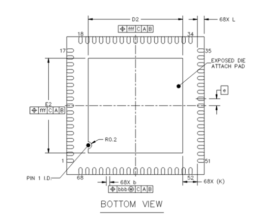
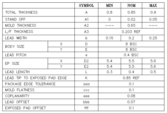
W55MH32L package

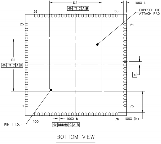

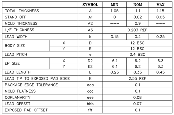
W55MH32Q package